


I. INTRODUCTION
Fractal means broken or irregular segments, which have self-similarity or self-affinity within their geometrical structure [Reference Mandelbort1]. Fractals can be applied for antenna design to achieve size miniaturizing, multiband and wideband characteristics [Reference Gianvittorio and Rahmat-Samii2]. Different Fractal shapes such as Koch snowflake, Sierpinski Gasket, Hilbert curve have been used for designing antenna over a period of time [Reference Werner and Ganguly3]. In today's world, reduced size antenna with wideband and multiband behavior are becoming most important design considerations for making things more and more compact with wide range of practical applications. Various size reduction techniques having wideband behavior using parasitic elements [Reference Iqbal, Siddiqui and Guha4], shorted pins, shaped slots [Reference Augustin, Bybi, Sarin, Mohanan, Aanandan and Vasudevan5, Reference Dehbashi6] or post-gap [Reference Guha and Siddiqui7], Coplanar waveguide feed [Reference Ghatak8] etc. came over a period of time, but all these have some disadvantages such as poor efficiency, high-cross polarization, low gains, and low bandwidth etc.
In contrast to conventional geometries of Koch, Sierpinski gasket and the Hilbert curve, new fractal shapes are emerging having more simple design, which are quite straight forward and easy to implement [Reference Bayatmaku, Lotfi and Azarmanesh9, Reference Weng and Hung10]. In our study, a new X-shaped fractal is proposed with defected ground structure (DGS) to design a multiband and wideband planar antenna. Proposed antenna is the combination of simple X-shaped fractal patch with ground plane having three vertical “I” shaped defects/slots to have size reduction and to control the flow of current on the antenna surface. The dimensions of slots are optimized to improve the antenna parameters such as impedance bandwidth and return loss. DGSs or slotted ground planes have been used to provide multi-band performance with size reduction in antennas [Reference Khanna, Kaur and Machavaram11, Reference Khanna and Parkash12]. DGS is achieved by etching defects on the ground plane of microstrip antenna, which perturbed the shield current distributions in the ground plane, influencing the input impedance and current flow of the antenna. In this DGS technique, the metallic strip of ground plane is intentionally modified for enhancing the performance of antenna [Reference Sharma, Kandwal and Khah13, Reference Kumar, Shinde and Upalne14]. The antenna is excited using a coaxial feed line of 50 Ω. Reflection coefficients |S 11| and three-dimensional (3D) radiation patterns shows the multi-band and wideband feature of the proposed X-fractal antenna with good directive gain.
The paper is organized as follows. Section I gives the introduction and literature review. Section II describes the mathematical background of X-shape fractal. Section III gives the design parameter of proposed antenna. Results and discussion are presented in Section IV and Section V presents the conclusion.
II. MATHEMATICAL BACKGROUND OF X-SHAPED FRACTAL WITH MICROSTRIP FEED LINE
In this section, the design methodology of proposed X-shaped fractal geometry is discussed. Figure 1 shows the design process of the proposed fractal shape. Initially at stage-1, it consists of two perpendicular metal strips both having length and width of L 1 and W respectively. The width of all metal strips remains unchanged in all stages. In stage-2, the length of the two perpendicular strips (L 2) is m × L 1, where m is the scale factor whose value lies between 0 and 1. Hence, L 2 is smaller than L 1. For stage-2, four pairs of these X-shaped perpendicular strips of length L 2 and width W are then added on all four corners of X of stage-1. The same procedure is applied in next two stages (i.e. third and fourth stage). Finally, the proposed X-shape fractal is achieved at stage-4 as shown in Fig. 2. The length of perpendicular strips of i th stage can be determined by the following expression:
 $$L(i + 1) = m\; L(i)\quad (i = 1,\; 2,\; 3),$$
where, m is multiplying factor and i is iteration number and L 1 is the initial length considered.

Fig. 1. Different stages of X-shaped fractal antenna. The proposed shape is at the stage-4.
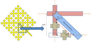
Fig. 2. Geometry of proposed antenna shape.
Different feeding techniques like microstrip feed line, coaxial feed line, proximity coupled, aperture coupled etc. can be used to use this X-shaped fractal as antenna. Special care should be taken in designing the geometry of antenna, while giving power using microstrip line feed so that its strips do not overlap with the feed line or they do not form any closed structure due to overlapping after any iteration.
Therefore, before designing the antenna with this X-shaped fractal, we have derived the condition of no overlapping between strips edges and microstrip feed line. In Fig. 3, the geometry of proposed antenna shape along with one portion zoomed is given, which is required to derive this condition. For simplicity and more clarity, intermediate stages L 2 and L 3 are not shown in Fig. 3.

Fig. 3. The dimensions of the proposed antenna at stage-4. (a) Front view, (b) back view.
It is clearly visible from Fig. 3, that in order to avoid overlapping between strips edges and microstrip feed line, the length AC must be greater than the length DE, i.e.
 $$AC\; \gt \; DE$$
From triangle ABC and DBE and with the help of Pythagoras theorem, (2) can be written as –
 $$AB\sqrt 2 \; \gt \; BE\sqrt 2. $$
After substituting the value of AB and BE in terms of L 1, W, and W 0, (3) becomes –
 $$\left( {\displaystyle{{L_1} \over 2} - \displaystyle{W \over 2} - \displaystyle{{W_0} \over {\sqrt 2}}} \right)\sqrt 2 \; \; \; \gt \; \; \left( {\displaystyle{{L_2} \over 2} - \displaystyle{W \over 2} + \displaystyle{{L_3} \over 2} + \displaystyle{{L_4} \over 2} + \displaystyle{W \over 2}} \right)\sqrt 2 \; \;, $$
where, W is the width of strip line.
Now, after substituting the value of L 2, L 3, and L 4 in terms of L 1 as given in (1), and (4) can be written as
 $$1 - m - m^2 - m^3 \gt \displaystyle{W \over {L_1}}\left( {1 + \displaystyle{{W_0} \over W}\sqrt 2 \;} \right)\; \;. $$
The above expression (5) can be generalized for N th stage to determine the range of scale factor m to avoid the overlapping:
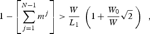 $$1 - \left[ {\mathop \sum \limits_{j = 1}^{N - 1} m^j} \right] \gt \displaystyle{{W_\;} \over {L_1}}\; \left( {1 + \displaystyle{{W_0} \over W}\sqrt 2 \;} \right)\; \;, $$
where, N is the stage number, W 0 is the width of feed line and L 1 is the initial length of strip lines at stage-1.
III. ANTENNA DESIGN
The dimensions of proposed antenna based on fractal shape as discussed in Section-II are given in this section. The resonance and impedance can be greatly affected by scale factor m (as it can control the size of the antenna), width of ground plane, number of slots in ground plane and their lengths; hence we can change theses different parameters for getting desired results.
In our proposed antenna, the width of all metal strips is taken identical as 3.0 mm. Microstrip feed line coupling used with the width of feed line is W 0.The geometry of the X-shape fractal is symmetric to the 50 Ω microstrip fed line. The dimensions of the ground plane are L g × W g . The thickness of substrate (T) is 1.6 mm. Other dimensions of the proposed antenna are listed in Table 1.
Table 1. Dimensions used in the proposed X-shaped fractal antenna.

As it is known that m must be a real number whose value lies between 0 and 1, the following condition is obtained after substituting the value of W, W 0, and L 1 (as given in Table 1) in (6)
 $$m \lt 0.5029$$
For the simplicity of design we have taken m = 0.5 in this paper.
IV. RESULTS AND DISCUSSIONS
In this section, the simulation results of proposed antenna are discussed and compared with the experimental results obtained after the fabrication of antenna. In the proposed antenna, patch and ground plane are made up of copper (annealed) of 0.07 mm thickness, electric conductivity of 5.8 × 10⁷ and is fabricated on FR4 substrate, with substrate thickness of 1.6 mm, dielectric constant of 4.4, and loss tangent of 0.02. The parametric results of following cases are discussed:
-
(a) Proposed structure at different stages (Stage-1–4) with constant width of ground plane.
-
(b) Variation in the width of ground plane of proposed antenna (at stage-4).
-
(c) Proposed antenna with DGS (having slots in ground plane).
-
(d) Proposed antenna with reduced feed line length and net reduction in total size
A) X-shaped fractal patch antenna with different stages of patch having constant width of ground plane
To observe the variation in resonant frequency, the reflection coefficient |S 11| is investigated by designing and simulating different stages of X-shaped fractal geometry with the help of simulator, CST MICROWAVE STUDIO 2014. Figure 4 shows the results of reflection coefficient |S 11| for four different stages (Stage-1–4), with width of ground plane W g as 20 mm as shown in Fig. 2. It can be easily observed from the graph that as the number of stages increases, the number of bands with |S 11 < −10 dB| also increases and as we approach to stage-4, the antenna shows more multiband and wideband behavior. The reason of multiple resonances is the increase in paths and lengths of the antenna geometry. The proposed structure can also be designed beyond the stage-4, but it roughly doubles the antenna size as compared with 4th stage, which is practically difficult to use.

Fig. 4. Reflection coefficients of the proposed X-fractal antenna in different stages.
B) X-shaped fractal patch antenna with different width of ground plane
Further, to optimize the characteristics of proposed antenna, the width of ground plane is varied and reflection coefficient for various cases has been studied. Figure 5(a) shows the reflection coefficient curve with different width of ground plane (vary from 4 to 28 mm with minimum variation of 4 mm). It is clearly visible from Fig. 5(a), that the proposed antenna structure can be fabricated with any particular ground plane width as it is giving multiband behavior for all the cases.

Fig. 5. Reflection coefficients of the proposed X-fractal antenna for different width of ground plane, (a) W g is 4, 8, 12, 16, 20, 24, 28 (b) W g is 5, 6, 7.
However, the better results are obtaining from W g = 4–8 mm. Therefore, we have further investigated the antenna by varying the width of ground plane from 5 to 7 mm and obtained its reflection coefficient curve as shown in Fig. 5(b). It is visible from Fig. 5(b) that the best results are obtained with W g = 6 mm. The antenna structure with W g = 6 mm is shown in Fig. 6.

Fig. 6. (a) Front view, (b) back view of proposed antenna with W g = 6 mm.
C) X-shaped fractal patch antenna having slots in ground plane
The results are further optimized using the slots in ground plane. Figure 7 shows the patch and ground plane of width 6 mm having three slots into it. Further, design and simulation of antenna is carried out for different value of slots length in the ground plane for optimized reflection coefficient value. Figure 8 shows the reflection coefficient value for the slot length of 2, 3, and 4 mm in the ground plane. It can be seen that, by cutting the slots of 4 mm in ground plane, the net electrical length increases without changing the input impedance of antenna as shown in smith chart in Fig. 9.

Fig. 7. (a) Front view, (b) back view of X-fractal antenna with three slots in 6 mm ground plane.

Fig. 8. Reflection coefficients of the proposed X-fractal antenna for three slots in the ground plane of different length.

Fig. 9. Smith chart plot showing input impedance of 49.16 Ω.
Figure 10 shows the photograph of fabricated antenna having X-shaped fractal patch up to 4th iteration, a ground plane of 6 mm width having three slots of 4 mm length. Measurement of results is carried out by E5071C Network Analyzer.

Fig. 10. Photograph of (a) front and (b) back view of the fabricated antenna.
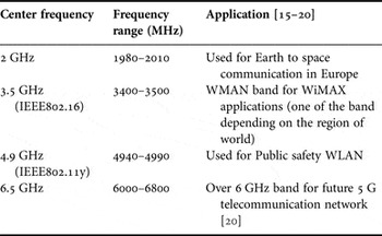
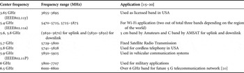
Figures 11 and 12 shows that the proposed antenna has good impedance match, directivity and radiation efficiency for the desired bands, covering various applications of L, S, and C Frequency bands as shown in Tables 2 and 3.
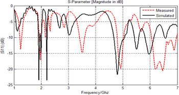
Fig. 11. Measured and simulated reflection coefficients of the proposed X-fractal antenna.

Fig. 12. Simulated 3D radiation patterns of the proposed X-fractal antenna for frequency (a) 2 GHz, (b) 3.5 GHz, (c) 4.9 GHz, (d) 6.5 GHz.
Table 2. Results of radiation patterns.
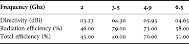
Table 3. Frequency bands and their applications.
D) X-shaped fractal patch antenna with reduced feed line length and net reduction in total size
To utilize wideband feature for practical application and to further reduce total size of antenna, the proposed X-shaped fractal antenna is further optimized by reducing the feed line length with DGS. Different values of feed line lengths are taken and results are carried out. Best optimized results are obtained for antenna having feed line length of 50 mm with net reduction in size of approximately 13% as compared with original antenna, as shown in Figs 13 and 14 (photograph of fabricated antenna with reduced size). Figure 15 shows the smith chart plot of the proposed antenna showing the input impedance value to be 49.11 Ω. Thus, maximum power will be transferred when Coaxial cable of 50 Ω characteristic impedance will be used for feeding the microstrip line.
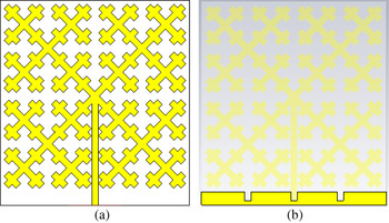
Fig. 13. (a) Front view (b) Back view of X-fractal antenna with reduced total size.
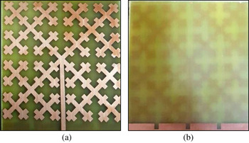
Fig. 14. Photograph of (a) front and (b) back view of the fabricated antenna with reduced size.
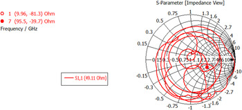
Fig. 15. Smith chart plot of the proposed antenna showing input impedance of 49.11 Ω.
The reflection coefficient value of simulated and fabricated antenna as shown in Fig. 16 shows a good wideband and multiband behavior of presented antenna. Figure 17 shows proposed antenna is also having good directivity and efficiency for the desired frequency bands, which covers various applications in S and C band as shown in Tables 4 and 5.

Fig. 16. Measured and simulated reflection coefficients of the proposed X-fractal antenna with reduced size.

Fig. 17. Simulated 3D radiation patterns of the proposed X-fractal antenna with reduced size for frequency (a) 3.6 GHz, (b) 5.5 GHz, (c) 5.95 GHz, (d) 6.5 GHz.
Table 4. Results of radiation patterns.

Table 5. Frequency bands and their applications.
V. CONCLUSION
In this paper, an X-shaped fractal patch has been proposed to design multiband antenna. Due to the simple structure of X-shaped fractal, it is easy to implement and fabricate antenna for practical use. Two different dimensions are given using proposed fractal shape patch for different application as mentioned in Tables 3 and 5. An exhaustive parametric study of proposed antenna has been done using both simulation and experimental methods. The experimental results were carried out using VNA and found to be closely matched with the simulations result. Based on the results, it is shown that we can have multiband and wideband behavior with proposed X-shaped fractal patch by changing its geometry, ground plane width, slot length and multiplying factor. Simulated 3D radiation pattern shows that proposed antenna have good directivity and efficiency for the desired bands. Optimized results show that we have achieved our desired goal of having various multiband and wideband applications in the required S and C band.
ACKNOWLEDGEMENTS
The authors would like to thank Dr. A. K. Singh and Dr. R. P. Yadav, Assistant Professor, Thapar University, Patiala for his useful suggestion and discussions regarding the proposed design. The authors would also like to thank Thapar University, Patiala for providing research facilities.
 Ankush Gupta received a Bachelor in Engineering degree from Thapar University, Patiala in 2014 and is pursuing Maters in Engineering from Thapar University in the field of Wireless Communication. He was with CSIR-CEERI, Pilani for 6 months for his Internship. His main research interests are design and optimization of Microstrip antenna design, Microwave Design, Fractal Antennas, Multiband and wideband antenna, and Wireless networks.
 Hem Dutt Joshi has completed his B.Tech. in ECE in the year July 1999 from Barkatullah University, Bhopal. He did his M.E. in Communication Control and Networking (CCN) from M.I.T.S., Gwalior in the year 2004. He worked as Assistant Professor in JUET, Guna from 2006 to 2013. Currently, he is working as Assistant Professor in Thapar Institute of Engineering and Technology, University, Patiala. His research include wireless communication systems, OFDM, MIMO-OFDM, Antenna designing. He is a life member of the Institution of Electronics and Telecommunications Engineers (IETE), India.
 Rajesh Khanna was born in Ambala, India. He received his B.Sc (Engineering) degree in Electronics & Communication in 1988 from REC, Kurkshetra and M.E degree in 1998 from Indian Institute of Sciences; Bangalore. He was with Hartron R&D centre till 1993. Until 1999 he was in All India Radio as Assistant Station Engineer. Presently he is working as Professor in the Department of Electronics & Communication at Thapar University, Patiala. He completed his Ph.D. degree in 2006. He has handled project worth Rs 95 lakhs and is presently handling projects worth Rs 70 lakhs, He has published 35 papers in SCI indexed international Journals and 20 Paper in International conferences. His area of interest includes wireless communication and Antennas. He has guided around 55 M.E. thesis and 11 Ph.D. thesis. Dr. Khanna is a Fellow of the Institution of Electronics and Telecommunications Engineers (IETE) and life member of ISTE, Punjab Academy of Sciences.


