


I. INTRODUCTION
Miniaturization of microstrip patch antenna is on demand to keep its importance in modern communication systems [Reference Wong1]. Microstrip patch antenna has several attractive features of small size, light weight, easy integration capability with circuits. Due to these advantages, microstrip patch antennas are used in portable devices such as mobile phones, laptops etc. [Reference Chen2]. The communication devices have shown a drastic reduction over the decade with respect to their size; henceforth the focus on compactness of microstrip patch antennas in these communication devices are on frontline of interest for various researchers [Reference Bhunia, Sarkar, Biswas, Sarkar, Gupta and Yasumoto3–Reference Kim, Jung, Ryu, Woo, Eun and Lee14].
The realization of compact multi frequency microstrip patch antenna has been reported by various authors in their articles using several techniques like cutting the slots on the patch, cutting slots on ground plane, monopole structure with defected ground plane, C shaped ring loading, using parasitic element etc. Bhunia et al. [Reference Bhunia, Sarkar, Biswas, Sarkar, Gupta and Yasumoto3] has investigated over compactness of microstrip patch antenna with the variation of slot length on the patch and he has found 85% size reduction with respect to conventional patch. He has also found 67% size reduction using unequal finger like slots on the patch [Reference Bhunia and Sarkar4]. Miniaturization of microstrip patch antenna by cutting the slots on the patch has been discussed in many more literatures [Reference Mahmoud and Baktur5–Reference Chakraborty, Kundu, Chowdhury and Bhattacharjee8]. Sarkar et al. [Reference Sarkar, Das Majumdar, Mondal, Biswas, Sarkar and Sarkar9] has proposed a new design of a miniaturized microstrip patch antenna with single slotted ground plane. Another technique of achieving multi frequency operation with monopole antenna structure and defected ground plane has been discussed in some articles [Reference Liu, Wu and Dai10–Reference Ellis, Zhao, Wu, Nie and Liu11]. Chen et al. [Reference Chen and Lin12] has proposed a novel miniaturized design of a microstrip fed slot antenna loading with a pair of C shaped ring inside a half wavelength slot and he has achieved 50% size reduction in this design. Mitra et al. [Reference Mitra and Chaudhuri13] has designed a compact microstrip patch antenna loading with a pair of split ring resonator and he has found 26% size reduction in comparison with slot antenna without split ring resonator. Kim et al. [Reference Kim, Jung, Ryu, Woo, Eun and Lee14] has proposed another new design of a compact multiband microstrip patch antenna using inverted L and T shaped parasitic element.
In this article a new approach of designing a compact multi frequency microstrip patch antenna has been proposed and experimentally verified. The proposed patch antenna with triangular slot and a pair of spur lines and strip loading offers multi frequency operation with 87% size reduction (with respect to the antenna, which is responsible to resonate at resonating frequency 1.8 GHz of the designed antenna). To calculate the size reduction the reference patch size is taken as the total area of the patch including strip line. The dimension of the ground plane is more than the four times the dimension of the patch so that it can be taken as infinite ground plane. It has been seen according to parametric study of designing of the antenna, that only spur lines are responsible for dual frequency, triangular slot introduces one extra frequency. In some previous works [Reference Lu, Yu and Wong15, Reference Lu and Wong16] it has been discussed that with the incorporation of spur lines microstrip patch antennas resonate at lower frequency. Combination of spur lines and strip loading generate much lower frequency than the frequency that generated due to spur lines or due to strip loading separately. The combination of spur lines, strip loading, and the triangular slot have shown much lower frequency as well as multi frequency operation, which causes a significant size reduction.
The performance comparison of the proposed antenna with some other designed antennas with respect to compactness and antenna dimension are shown in Table 1, respectively.
Table 1. Performance comparison of proposed antenna with other antenna with respect to compactness, dimension, and multi frequency.

Table 1 show that the proposed antenna has not only the largest compactness with respect to patch dimension but also it radiates multi frequency. It has been found from the above comparison that only the antenna designed in the paper [Reference Sarkar, Das Majumdar, Mondal, Biswas, Sarkar and Sarkar9] has more compactness but it is designed for single frequency. Our proposed antenna has maximum compactness and good gains with acceptable values among all the designed multi frequency antennas.
II. ANTENNA CONFIGURATION AND DESIGN CONCEPT
The width (W) and the length (L) of reference antenna (Antenna 1) are calculated from conventional equations discussed in literature [Reference Hammerstad17].
The length (L) and width (W) of the patch of reference microstrip antenna (Antenna 1) are 14 and 18 mm, respectively, with substrate (Arlon AD300A) of dielectric constant ε r = 3, thickness h = 1.524 mm, and loss tangent (tanδ) is 0.002. The ground plane is taken as infinite and microstrip patch has been fed by coaxial cable at optimum location to achieve characteristic impedance of 50 Ω. Figure 1 shows the schematic of reference patch antenna (Antenna 1). Figure 2 shows the geometry of reference patch antenna with spur lines (Antenna 2a). The reference patch antenna loaded with spur lines and triangular slot (Antenna 2b) is shown in Fig. 3. Figure 4 shows the schematic of reference patch with spur lines and single strips (Antenna 2c). The geometry of reference patch with spur lines and double strips loading (Antenna 2d) is shown in Fig. 5. The ground plane is taken as infinite and probe is fed at optimum location to get impedance matching. The effect of spur lines, triangular slot and strips loading has been realized individually from return loss versus frequency graphs of Antenna 2a, Antenna 2b, Antenna 2c, and Antenna 2d. Figure 6 shows the geometry of proposed antenna with triangular slot, spur lines, and strips loading (Antenna 3). The ground plane is taken as infinite. The probe is fed at the position shown in the Fig. 2 to get the optimum impedance matching. The design of the antenna is vertically symmetrical in nature. The fabricated Antenna 3 is shown in Fig. 7.
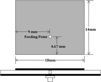
Fig. 1. Antenna 1 configuration.

Fig. 2. Antenna 2a configuration.

Fig. 3. Antenna 2b configuration.
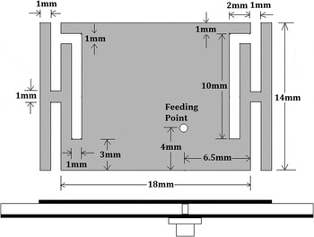
Fig. 4. Antenna 2c configuration.

Fig. 5. Antenna 2d configuration.
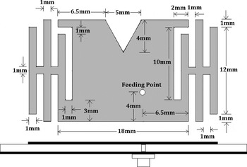
Fig. 6. Antenna 3 configuration.

Fig. 7. Fabricated Antenna 3 structure.
III. EQUIVALENT CIRCUIT
The equivalent circuits of all antennas are shown in Figs 8(a)–8(f). A conventional microstrip patch antenna can be modeled as a simple RLC resonant circuit shown in Fig. 8(a). The values of R, L, and C can be determined by the conventional formulae given in [Reference Shivnarayan, Sharma and Vishvakarma18].

Fig. 8. Equivalent circuit of (a) Antenna 1, (b) Antenna 2a, (c) Antenna 2b, (d) Antenna 2c, (e) Antenna 2d, and (f) Antenna 3.
After inserting the spur lines into the patch the resonant features changes as shown in Fig. 8(b). Due to insertion of spur lines one current flows like normal patch in the middle part of the patch, which represents the initial RLC circuit and resonates at its initial frequency and at the edge part of the patch the current has to flow around the spur lines as a result of increasing the length of the current path, which can be modeled as an additional series inductance ΔL 1 [Reference Yang, Zhang, Ye and Samii19]. So the equivalent circuit changes from a single resonant circuit to a double resonant circuit. The additional resonant circuit has greater inductance, which results the lower resonant frequency.
Antenna 2b configuration illustrates the patch with spur line and a triangular notch. The equivalent circuit for Antenna 2b is shown in Fig. 8(c). The resonant feature also changes with the incorporation of the triangular notch into the patch. In this case two currents flow in the patch; one is normal current that flows for any conventional patch and another meandered current around the notch and hence the current path increases [Reference Shivnarayan and Vishvakarma20]. In this case both the electric and magnetic field discontinuity occur across the notch. So the effect of notch will be both capacitive and inductive as shown in Fig. 8(c); these effects are modeled as additional series inductance ΔL 2 and series capacitance ΔC 2 to the equivalent circuit for Antenna 2b.
Antenna 2c configuration shows the patch with spur lines and a pair of strips. The strip loading affects the electric field discontinuities mostly over magnetic field discontinuities, which can be modeled by inserting an additional capacitance ΔC S1 in parallel with the equivalent circuit of Antenna 2a. The equivalent circuit for Antenna 2c is shown in Fig. 8(d). Due to this additional capacitance ΔC S1 the total capacitance of the resonant circuit increases, which results far lower frequency operation.
Similarly another extra strip will introduce another capacitance ΔC S2 in equivalent circuit for Antenna 2d, shown in Fig. 8(e). This extra capacitive effect again lowers the frequency for Antenna 2d than Antenna 2c.
The proposed Antenna 3 configuration shows the patch with spur lines, triangular notch and two pair of strips. The equivalent circuit is shown in Fig. 8(f) where all the effects of ΔL 1, ΔL 2, ΔC 2, ΔC S1, and ΔC S2 have been considered, which causes size reduction and multi frequency operation.
IV. PARAMETRIC STUDY
Huge simulation works are done with the antenna structure shown in Fig. 9 to find out the dimension of the different parameters for the best performance of the designed antenna. The results of these studies are shown in tables and in graphs below.

Fig. 9. Antenna with spur line, strips, and triangular slot.
Table 2 and Fig. 10(a) show that the optimum length of L S1 is 10 mm. Table 3 and Fig. 10(b) show that the optimum length of L S2 is 14 mm. Table 4 and Fig. 10(c) show that for L S3 = 14 mm the results of return loss and the resonant frequency are little better than L S3 = 12 mm but if the bandwidth is taken into consideration the optimum length of L S3 will be 12 mm, which has been taken to design the antenna. Table 5 and Fig. 10(d) show that the optimum length of L S4 is 4 mm. It has also been seen that instead of triangular notch if rectangular notch is used, the gain for the 2nd resonant frequency of the antenna drastically falls to 1 dBi from 5 dBi. The result of return loss is poor for rectangular notch.
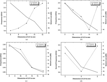
Fig. 10. (a) Frequency and return loss with variation of L S1. (b) Frequency and return loss with variation of L S2. (c) Frequency and return loss with variation of L S3. (d) Frequency and return loss with variation of L S4.
Table 2. Effect of resonant frequency and return loss with the variation of L S1 where L s2 = 14 mm, Ls3 = 12 mm, and L s4 = 4 mm (Fig. 9).
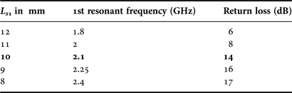
Bold values are optimum values among the other values of parametric studies and these bold values have been taken for designing of proposed antenna.
Table 3. Effect of resonant frequency and return loss with the variation of L S2 where L s1 = 10 mm, Ls3 = 12 mm, and L s4 = 4 mm (Fig. 9).

Bold values are optimum values among the other values of parametric studies and these bold values have been taken for designing of proposed antenna.
Table 4. Effect of resonant frequency and return loss with the variation of L S3 where L s1 = 10 mm, Ls2 = 14 mm, and L s4 = 4 mm (Fig. 9).
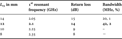
Bold values are optimum values among the other values of parametric studies and these bold values have been taken for designing of proposed antenna.
Table 5. Effect of resonant frequency and return loss with the variation of L S4 where L s1 = 10 mm, Ls2 = 14 mm, and L s3 = 12 mm (Fig. 9).
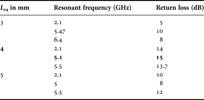
Bold values are optimum values among the other values of parametric studies and these bold values have been taken for designing of proposed antenna.
The gain variation of the antenna, shown in Fig. 9, with spur line length and strip lengths are shown in Figs 11(a)–11(c). It has been found that length of the spur lines as well as strip lines, which are taken for designing the proposed antenna are optimal.

Fig. 11. (a) Variation of gain with L S1. (b) Variation of gain with L S2. (c) Variation of gain with L S3.
V. RESULTS AND DISCUSSION
The return losses of all antennas were studied using method of moment-based commercially available software (IE3D) and return losses of all fabricated antennas were studied using vector network analyzer. The simulated results are shown in Table 6.
Table 6. Simulated results.
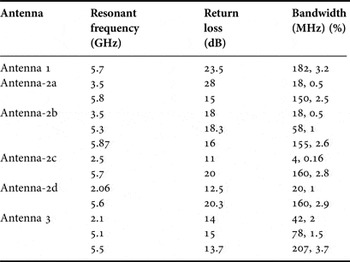
The measured results of Antenna 1 and proposed Antenna 3 are shown in Table 7.
Table 7. Measured results of Antenna 1 and Antenna 3.
The simulated and measured frequency versus return loss graphs for reference Antenna 1 is shown in Fig. 12 and the simulated frequency versus return loss graphs for Antenna 2a, Antenna 2b, Antenna 2c, and Antenna 2d are shown in Fig. 13. The simulated and measured frequency versus return loss graphs for Antenna 3 is shown in Fig. 14.

Fig. 12. Frequency versus return loss graph for Antenna 1.
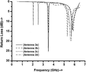
Fig. 13. Simulated frequency versus return loss graph for Antenna 2a, Antenna 2b, Antenna 2c, and Antenna 2d.
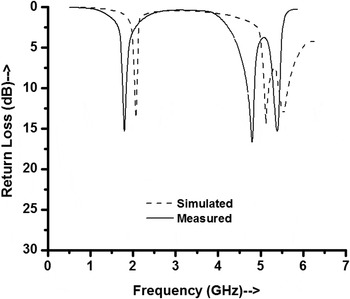
Fig. 14. Frequency versus return loss graph for proposed Antenna 3.
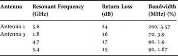
The simulated and measured radiation pattern for Antenna 1 and proposed antenna 3 are shown in Fig. 15. The simulated and measured gain, simulated radiation efficiency and directivity of proposed Antenna 3 are shown in Figs 16–18. The measured gain of the proposed Antenna 3 for frequencies 1.8, 4.7, and 5.4 GHz are 1.5, 5.8, and 6.2 dBi, respectively. Directivity and radiation efficiency (Simulated) at the frequencies 2.1, 5.1, and 5.5 GHz are 5, 6.8, 7.1 dBi, and 37, 81, and 84%, respectively.

Fig. 15. Simulated and measured radiation pattern for (a) Antenna 1 at 5.6 GHz, (b) Antenna 3 at 1.8 GHz, (c) 4.7 GHz, and (d) 5.4 GHz.

Fig. 16. Gain of Antenna 3.

Fig. 17. Radiation efficiency of Antenna 3.
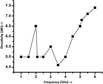
Fig. 18. Directivity of Antenna 3.
VI. CONCLUSION
New antenna structures with spur lines and strip loading have been studied in this paper. Due to incorporation of spur lines the current line paths have been lengthening, which causes lower frequency operation. Inserting triangular slot an additional resonating frequency has been obtained in addition to two frequencies, which have been found due to insertion of spur line only. Due to slot loading, capacitive loading has been increased, which has led to further frequency reduction. From the results of parametric study the optimum value of the length and width of strip and spur lines have been taken by considering the resonant frequency, return loss and gain to design the proposed antenna in this paper. Conventional Antenna 1 and proposed Antenna 3 have been simulated with the help of method of moment-based commercially available software (IE3D) and fabricated. The measured results have been compared with the simulated results and measured results have been found almost same with the simulated one. Multi frequency operation as well as size reduction of about 87% has been seen in Antenna 3, with respect to the patch antenna whose dimension is equivalent to the patch antenna with strip lines. The proposed antenna may be suitable for some wireless communication systems such as PCS (1.75–1.87 GHz), INSAT system (4.5–4.8 GHz), and WiMAX (5.25–5.85 GHz).
ACKNOWLEDGEMENTS
Authors are grateful to Department of Science and Technology, Government of India for supporting research grant under Young Scientist Scheme by Dr. Sunandan Bhunia vide sanction no. SERB/F/2012/ 2012–2013 dated 11/07/2012.
 Avisankar Roy received his B.Tech. and M.Tech. degree in Electronics and Communication Engineering from Maulana Abul Kalam Azad University of Technology (formerly known as West Bengal University of Technology), WB, India, in the year 2006 and 2009, respectively. His area of research interest includes Microstrip Antenna design and Frequency Selective Surfaces. He has contributed to numerous research articles in various journals and conferences of repute. He is working towards his Ph.D. degree.
 Sunandan Bhunia obtained his B.Tech. and M.Tech. from Institute of Radiophysics and Electronics, Calcutta University in 2002 and 2004, respectively. He obtained Ph.D. degree in Engineering from Jadavpur University in 2009. He was awarded gold medal from Vidyasagar University for 1st class 1st in Physics (H) in 1999. He is currently working as Associate professor in the department of Electronics and Communication Engineering, Central Institute of Technology, BTAD, Assam. He has published about 40 research article in reputed international & national journal and conferences. His area of research interest includes, Microstrip Antenna, Microstrip Filter, and Frequency Selective Surfaces, VLSI etc.
 Debasree Chanda Sarkar was felicitated with a Ph.D. in Engineering from Jadavpur University in the year 2005. She has obtained her M.E. from Bengal Engineering and Science University, Shibpur in the year 1994. She earned her B.E. degree in Electronics and Telecommunication Engineering from Bengal Engineering College (presently known as IIEST, Shibpur) in the year 1991. She is presently working as Scientific Officer (Associate Professor Rank) at the Department of Engineering and Technological Studies, University of Kalyani. Her area of research includes, Microstrip Antenna, Microstrip Filter, Frequency Selective Surfaces, and Artificial Neural Network. She has contributed to numerous research articles in various journals and conferences of repute.
 Partha Pratim Sarkar was felicitated with a Ph.D. in Engineering from Jadavpur University in the year 2002. He has obtained his M.E. from Jadavpur University in the year 1994. He earned his B.E. degree in Electronics and Telecommunication Engineering from Bengal Engineering College (presently known as IIEST, Shibpur) in the year 1991. He is presently working in the rank of Professor at the Dept. of Engineering & Technological Studies, University of Kalyani. His area of research includes, Microstrip Antenna, Microstrip Filter, Frequency Selective Surfaces, and Artificial Neural Network. He has contributed to numerous research articles in various journals and conferences of repute. He is also a life Fellow of IETE and IE(India).
 Santosh Kumar Chowdhury obtained his Ph.D. in Engineering from Jadavpur University in the year 1971. He has obtained his M.E. from Jadavpur University in the year 1968. He earned his B.E. degree in Electronics and Telecommunication Engineering from Jadavpur University in the year 1964. He is a Senior Member of IEEE, Life fellow of IETE, Fellow of IE, Fellow of West Bengal Academy of Science and Technology. His area of research includes, Microstrip Antenna, Microstrip Filter, and Frequency Selective Surfaces. He has contributed more than 200 international research articles in various journals and conferences of repute.


