


Introduction
Modern radio frequency Systems-on-Chip (RF SoCs) have become increasingly complex, integrating both RF and digital circuits to achieve high performance within a smaller area and at a lower cost. While this integration offers numerous advantages, it also introduces a major challenge: interference between RF and digital subsystems [Reference Raskin, Viviani, Flandre and Colinge1]. The switching activity of digital circuits generates parasitic signals that can leak into the substrate and couple to sensitive RF front-end components, such as voltage-controlled oscillators (VCOs). This coupling can degrade spectral purity, increase phase noise, and induce frequency pulling, ultimately compromising the VCO’s performance. The extent of this interference is strongly influenced by the substrate’s conductivity, making it a critical factor in RF SoC design. This issue, commonly known as the substrate noise problem in VCOs, has been extensively studied in the literature.
For example, in Azuma et al. [Reference Azuma, Shimazaki, Miura, Nagata, Kitamura, Takahashi, Murakami, Hori, Nakamura, Tsukamoto and Iwanami2], substrate noise coupling from a digital arbitrary noise generator to a 65 nm CMOS RF receiver front end for long-term evolution (LTE) wireless communication was observed, confirming that leaking noise from digital circuits can propagate through the substrate and create unwanted spurs in RF bands. In Kousai et al. [Reference Kousai, Agawa, Ishikuro, Majima, Kobayashi, Miyashita, Yoshino, Hama and Hamada3], the authors showed that digital noise couples to RF parts of a Bluetooth SoC and causes a degradation of its spectral purity along with its phase noise. Since these problematic noise signals propagate through the shared silicon substrate, the issue could be strongly mitigated by having a proper high-resistivity (HR) substrate, as suggested in Bendou et al. [Reference Bendou, Rack, Lederer, Cathelin and Raskin4], where simulations were made to quantify the effect of the silicon substrate resistivity on parasitic spurs appearing in a VCO’s output spectrum.
Traditional techniques for mitigating substrate noise coupling in VCOs, such as guard rings and deep N-well (DNW) isolation [Reference Afzali-Kusha, Nagata, Verghese and Allstot5, Reference Checka, Wentzloff, Chandrakasan and Reif6], offer only partial solutions and present significant limitations. Guard rings can divert noise away from sensitive circuits, but they become less effective at high frequencies due to parasitic capacitance and consume valuable silicon area. DNW isolation reduces direct noise coupling by creating an electrically isolated region, but it still allows coupling through capacitive and resistive paths and introduces additional design complexity. Moreover, both techniques primarily attempt to contain or divert noise rather than fundamentally suppressing its propagation. In contrast, HR substrates offer a more effective solution by inherently increasing substrate impedance, thereby reducing noise transmission at its source [Reference Raskin, Viviani, Flandre and Colinge1].
In this work, VCOs were designed in the 28 nm FD-SOI CMOS technology from STMicroelectronics, each with its neighboring metallic pad for substrate noise injection. They were fabricated on process-of-reference (POR) wafers presenting a handle silicon substrate resistivity of 10 Ω.cm and also on 1 kΩ.cm HR Si wafers. To the best of the author’s knowledge, this is the first time VCOs were fabricated on HR silicon handle substrate in the 28 nm FD-SOI technology to investigate the impact on substrate noise coupling. Indeed, VCOs are critical RF blocks that are expected to deliver the purest possible signal to other blocks on the chip,which can be challenging in the presence of substrate noise. An earlier version of this paper was presented at the EuMW2024 conference and was published in its proceedings [Reference Bendou, Lederer, Cathelin and Raskin7]. This extension adds a theoretical analysis as an introduction and motivation behind using HR substrates to mitigate substrate noise coupling for VCOs, as well as a deeper explanation of parasitic surface conduction (PSC) and the use of PN junctions and field-effect passivation to mitigate the PSC. A more elaborate explanation of the inductor differences between the two versions of VCOs designed is also provided accompanied with a better visual representation of the inductors in 3D. It also elaborates more on the layout of the two passivation methods used to combat the PSC when implemented for a VCO. A simulation of the substrate transfer function  ${H_{sub}}$ as a function of the type of substrate is included along with a description of the simulation methodology. In terms of measurement results, measurements of the VCO’s main inductors are included for two types of substrates and all other measurements previously provided in the original paper now include the FE-passivated VCO too. In addition, previous figures and text are upgraded to provide a better understanding and quality compared to the original paper.
The paper is organized as follows: first, substrate noise mechanisms and their link to the use of HR substrate as a mitigator are discussed in “Substrate noise for voltage-controlled oscillators” section. The section “High-resistivity substrate in FD-SOI technology” describes the tested HR substrates, explains the parasitic surface conduction (PSC) issue and the passivation techniques used in this work to mitigate that effect. The section “VCO design” presents the VCOs designed as test vehicles for this study. The section “Simulation methodology and results” describes the simulation methodology and shows the substrate transfer function simulation results. The section “Measurement result” shows measurement results of the inductors as stand-alone structures, the typical figures-of-merit (FoMs) of the VCOs such as phase noise and the tuning range, and measurement results of noise coupling as a function of the type of silicon substrate used. Finally, the “Conclusion” section summarizes the results and concludes about the use of HR FD-SOI substrates to mitigate the substrate noise problematic.
Substrate noise for VCOs
The subject of substrate noise impacting VCOs is well-studied in the literature [Reference Azuma, Shimazaki, Miura, Nagata, Kitamura, Takahashi, Murakami, Hori, Nakamura, Tsukamoto and Iwanami2–Reference Singh and Sharma10]. It is usually divided into three main categories: noise generation, propagation, and impact (Fig. 1). In this work, the main focus is on the propagation part, on which the impact of raising the substrate resistivity is studied. Indeed, the substrate can be viewed as an RC network linking any two points on top of its surface, such that a substrate transfer function  ${H_{sub}}$ can be associated to it.
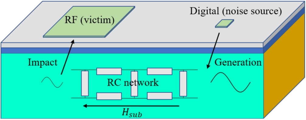
Figure 1. Noise coupling mechanism through the substrate.
The oscillator free-running frequency  ${f_c}$ depends on the control voltage
  ${V_{control}}$ such that a VCO sensitivity function can be defined as follows:
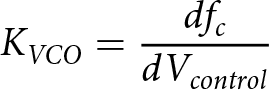 \begin{equation}{K_{VCO}} = \frac{{d{f_c}}}{{d{V_{control}}}}\end{equation}
This equation can be generalized as in Equation (2) for any voltage present at some node i of the VCO, including substrate noise signals that propagate through the substrate to reach and enter into the VCO via different nodes.
 \begin{equation}{K_i} = \frac{{d{f_c}}}{{d{V_i}}}\end{equation}
The signals coming from the same noise source reaching the VCO through the substrate are small signals and can be expressed as:
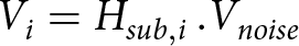 \begin{equation}{V_i} = {H_{sub,i}}\,.{V_{noise}}\end{equation}
  ${H_{sub,i}}$ being the transfer function from the noise source to the substrate node i, and
  ${V_{noise}}$ the substrate noise voltage at the source with an amplitude
  ${A_{noise}}$ and frequency
  ${f_{noise}}\,$:
 \begin{equation}{V_{noise}}\left( t \right) = {A_{noise}}.{\text{cos}}\left( {2\pi {f_{noise}}t} \right)\end{equation}
Substrate noise here is being represented by a single tone frequency signal that will be injected into the substrate through a dedicated pad located in the vicinity of the VCO in order to study the impact of the substrate resistivity on the rejection of unwanted spurs near the carrier frequency.
Since the substrate noise signals are orders of magnitude smaller than the VCO’s main signal, superposition can be assumed, such that each one of the  ${V_i}$ voltages contributes to the frequency modulation (FM) of the VCO carrier frequency
  ${f_c}$ following the expression [Reference Soens, Van der Plas, Wambacq, Donnay and Kuijk8]:
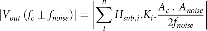 \begin{equation}\left| {{V_{out}}\left( {{f_c} \pm {f_{noise}}} \right)} \right| = \left| {\mathop \sum \limits_i^n {H_{sub,i}}.{K_i}.\frac{{{A_c}\,.\,\,{A_{noise}}}}{{2{f_{noise}}}}} \right|\end{equation}
  ${A_c}$ is the amplitude of the VCO’s main signal. Equation (5) shows that the spur generated because of the noise signal at frequency
  ${f_c} \pm {f_{noise}}$ has an amplitude proportional to the sum of the products between the substrate transfer function
  ${H_{sub,i}}$ from the noise source to node i, and the VCO sensitivity function
  ${K_i}$ related to the voltage at the same node i. The former is directly related to the substrate’s conductive properties and the latter depends on the VCO architecture and design itself. The nature of the solution used in this work does not necessitate a change in the design of the VCO, only in the substrate properties to reduce
  ${H_{sub,i}}$ and therefore minimize the power of the parasitic spurs at
  ${f_c}\, \pm\, {f_{noise}}$. Simulations illustrating those dependences are shown in the section “Simulation methodology and results”.
High-resistivity substrate in FD-SOI Technology
Raising the resistivity of a silicon substrate is beneficial to RF circuits, mainly due to its low-loss nature and its reduction of harmonics generation [Reference Rack and Raskin11, Reference Neve and Raskin12]. However, it is also known that HR Si substrates in SOI technologies suffer from parasitic surface conduction (PSC) as illustrated in Fig. 2(a) [Reference Wu, Gamble, Armstrong, Fusco and Stewart13, Reference Lederer and Raskin14], a phenomenon occurring due to the nature of the CMOS SOI process. Indeed, the buried oxide (BOX) layer, located beneath the top Si thin film where the transistors are implemented, contains fixed positive charges that attract electrons from the handle Si substrate creating a vertical gradient of resistivity with a quite low-resistivity value (only a few mΩ.cm) at the interface with the BOX. This translates to an effective resistivity, resistivity sensed by the passive and active devices integrated on top of the substrate [Reference Lederer and Raskin14], of only a few tens of Ω.cm despite having a handle Si substrate characterized by a nominal resistivity larger than 1 kΩ.cm.
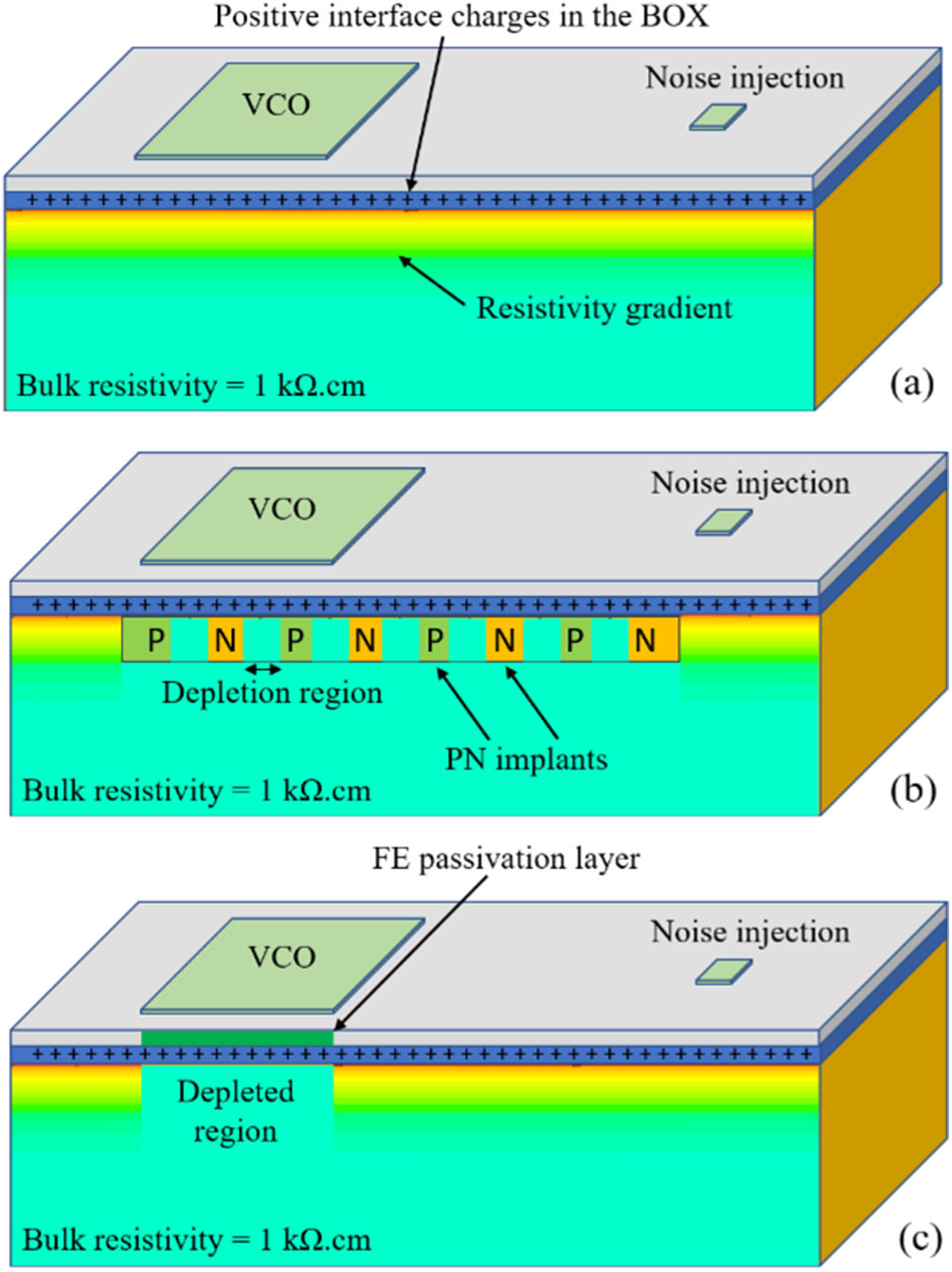
Figure 2. HR-SOI substrates and passivation solutions. (a) No passivation. (b) PN implants passivation. (c) Field effect, and (FE) passivation.
Trap-rich (TR) SOI substrate is a commercially available solution to the PSC problem, with the eSI wafers from the company SOITEC for the PD-SOI technology. It offers improved isolation and reduces substrate losses. However, it is not compatible with the below-the-BOX function of the FD-SOI technology which is the back-gate of transistors. To preserve the back-gate function of FD-SOI transistors, a more locally implementable solution is needed. This would give the designer more flexibility to raise the resistivity of the substrate in areas that are judged to be critical, such as the substrate areas under passives or around transistor interconnects without disrupting the transistor function.
One solution proposed in the literature to mitigate this problem and used in our study relies on the implantation of a series of PN junctions directly beneath the oxide layer (Fig. 2(b)) [Reference Rack, Nyssens and Raskin15, Reference Nyssens, Rack, Nabet, Schwan, Zhao, Lehmann, Herrmann, Henke, Kondrat, Soonekindt and Koch16]. The implantation step below the BOX is an already existing process step of the FD-SOI process for the definition of the back-gate contact, so no modification of the process is needed. This creates a horizontally alternating resistivity profile at the surface underneath the oxide, with low resistivity regions for the P- and N-doped pockets and very HR for the depletion at each junction. Thanks to the creation of depletion junctions beneath the BOX, the effective resistivity of the substrate achieves values close to the HR nominal resistivity as demonstrated in [Reference Rack, Nyssens and Raskin15]. The PN junctions can be reverse-biased for further increasing the substrate effective resistivity [Reference Nyssens, Rack, Nabet, Schwan, Zhao, Lehmann, Herrmann, Henke, Kondrat, Soonekindt and Koch16]. As presented in the section “VCO design”, ring-like annular disposition of PN junctions around the sensitive parts of the circuit are used in this work and their efficiency to reduce substrate noise coupling is studied. We also propose another solution to mitigate the PSC problem that we call field-effect (FE) passivation (Fig. 2(c)). It relies on the application of a bias on the thin active silicon layer of the SOI technology that is above the BOX, to induce an electric field at the BOX-Si interface, effectively depleting charge carriers and preventing the formation of a conductive layer at that interface. The thin Si film electrode comes with the SOI substrate therefore no modification of the process is needed. As demonstrated in the section “Measurement results”, the FE passivation technique significantly increases the effective resistivity of the substrate and thus improves the quality factor of passive elements such as inductors and minimizes the substrate noise.
The PSC passivation solutions proposed here can be implemented locally. Additionally, both solutions use layers already present in the FD-SOI process physical design kit, making them cost-effective and reliable. Figures representing the layout of the circuit along with the passivation solutions are shown in the section “VCO design”.
VCO design
VCO layout: POR vs HR
Four VCOs were designed for this study. One for each type of substrate variant and passivation technique (Fig. 3). POR refers to the VCO issued from the process of reference with a standard substrate resistivity (around 10 Ω.cm), whose layout is optimized for such substrate. PSC, PN, and FE, respectively, refer to the VCOs optimized for HR substrates, without passivation thus suffering from PSC, with the PN implants passivation solution, and with the FE passivation technique.

Figure 3. Depiction of the four VCOs designed and taped-out for this study.
All VCOs have the same LC tank architecture with a cross-coupled pair of SLVT NMOS transistors that replenish the losses in the LC tank and a pair of SLVT NMOS varactors serving as variable capacitors (221fF to 450fF) to tune the frequency of the circuit using a control voltage to be able to cover the targeted frequency band 14–16 GHz (Fig. 4). The output is also buffered to isolate the VCO and to reduce frequency pulling effects from the load at the output.
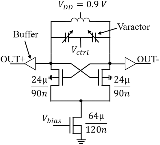
Figure 4. LC tank VCO architecture.
The circuits also have the exact same chip layout except for the inductor which is differently optimized for the POR and the HR substrates (Fig. 5). In the POR substrate variant of the VCO, the inductor is built using the two top metal layers for the spiral track and the lower-level metal to shield the inductor from the lossy 10 Ω.cm substrate. In the three other variants based on a 1 kΩ.cm HR Si substrate, the substrate losses being strongly minimized we can profit from the rich back-end of line and stack the three top metal layers to reduce series resistance and thus significantly improve the inductor quality factor (Q). Adding an additional metal layer changes the inductance value and thus its geometry must be changed to get the same inductance value than in the POR case for comparison purposes. As illustrated in Fig. 5, the dimensions of the inductor on HR substrates are a diameter  $D = 275\,\mu m$ and a track width
  $W = 20\,\mu m$ while
  $D = 270\,\mu m$ and
  $W = 22.5\,\mu m$ for the inductor on the POR substrate.
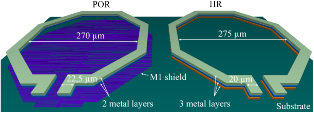
Figure 5. Stand-alone inductors used in the two types of VCOs.
PN and FE passivation layout
The passivation solutions must be well implemented below the passives like inductors and CPW lines and around the transistors and active parts of the circuits which could be sensible to substrate noise injection.
The PN passivation solution which consists of series of PN junctions characterized by an alternating resistivity profile must be placed perpendicular to the direction of the coupling electric field penetrating into the substrate in order to raise the impedance along the electric field path. Figure 6 shows the implementation of the PN junctions in the case of a CPW line and an inductor.

Figure 6. Implementation of PN junctions passivation in the case of a CPW line and an inductor. (a) Top view for a CPW line. (b) 3D view for a CPW line. (c) Top view for an inductor.
For the VCO used in this work, the PN junctions are placed under the inductors following the metal track from underneath, as well as all around the active part (transistor region) and the full circuit in ring shapes as shown in Fig. 7. The PN junction lines shown in the figure are not shown on scale for representation and simplicity purposes.

Figure 7. VCO layout with PN passivation.
The PN lines put underneath the inductor help increase the effective resistivity in the substrate region around the inductor, therefore reducing substrate losses and enhancing its quality factor [Reference Nyssens, Rack, Nabet, Schwan, Zhao, Lehmann, Herrmann, Henke, Kondrat, Soonekindt and Koch16]. The PN lines put around the active part and around the whole circuit increase the resistance of the substrate path for the noise signals reaching the VCO, effectively improving the isolation of the VCO on HR substrates. These PN lines are also connected to two DC pads, allowing the application of a reverse bias that further increases the width of the depletion regions, therefore raising even more the effective resistivity of the substrate.
FE passivation follows a similar logic to the PN passivation, as it is not only placed following the inductor track from underneath but also around the active part and the whole circuit, as shown in Fig. 8.
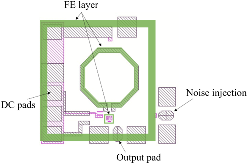
Figure 8. VCO layout with FE passivation.
The FE layer is connected to a DC pad to be able to apply the correct voltage  ${V_{FE}}$ that depletes the interface beneath the BOX. This voltage
  ${V_{FE}}$ changes from a process to another as it depends on the oxide charge
  ${Q_{OX}}$ present in the BOX which is a process-dependent variable.
Simulation methodology and results
Simulation methodology
The layout of the VCO is divided into two parts: a first part which contains all the passives, on-chip interconnects, and the substrate, and a second part that only includes the active devices and a few lower-level metals in their vicinity. The first part was simulated using ADS Momentum, by choosing a different substrate resistivity profile for each case (10 Ω.cm, 1 kΩ.cm with PSC, and 1 kΩ.cm). The second part was simulated using the Quantus parasitics extraction (PEX) tool. The results of the two simulations were then properly coupled together on the same testbench to fully capture the substrate effects under investigation. The final testbench was created using an S-parameter box resulting from the ADS Momentum simulations, together with the model of the transistors extracted using Quantus PEX. After having connected all the nodes together, an AC analysis was performed from 1 MHz to 1 GHz to extract the substrate transfer function from the noise source to a pin defined in the ADS Momentum simulation, located near the active part of the layout containing the transistors of the VCO. The PSC substrate profile was defined in ADS Momentum by combining the results of TCAD simulations along with Momentum’s substrate definition interface [Reference Bendou, Rack, Lederer, Cathelin and Raskin4]. TCAD simulations of a highly resistive FD-SOI substrate determine the vertical carrier concentration profile  $\rho \left( z \right)$ along the thickness of the substrate and this allows the designer to make segments and discretize the
  $\rho \left( z \right)$ function to be able to input it in the ADS Momentum substrate definition interface [Reference Rack17].
Substrate transfer function simulation results
As seen in Equation (5), the amplitude of the parasitic spurs generated at the output of the VCO because of the injection of a substrate noise signal is proportional to the substrate transfer function  ${H_{sub}}$. Figure 9 summarizes the simulation results for
  ${H_{sub}}$ when different substrate resistivity profiles are considered.

Figure 9. Simulated  ${H_{sub}}$ as a function of frequency for different SOI substrates.
Figure 9 shows that moving from POR substrate to HR SOI, without using any passivation technique, leads already to a reduction by 10–15 dB of  ${H_{sub}}.$ As discussed, the HR substrate suffers from PSC effect and thus its effective resistivity is lower than the base nominal resistivity of 1 kΩ.cm, and is also quite dependent of the oxide-Si substrate interface quality which is process and foundry dependent. Whereas for the passivated HR substrate the effective resistivity is close to 1 kΩ.cm and pretty process independent. This translates to a minimum substrate coupling with
  ${H_{sub}}$ reduced by approximately 25 dB compared with the POR substrate.
Measurement results
The four VCOs were fabricated on each type of substrate (Fig. 10), and measured. The POR VCO was measured on a standard resistivity wafer while the other three VCOs were measured on a HR wafer. Output power, frequency of oscillation, phase noise, and output spectrum were measured using a Keysight E505xA Signal Source Analyzer. Noise injection into the substrate was performed using an Agilent E8267D Vector Signal Generator. The inductors used in the LC tank of the VCOs were also measured in a small signal S-parameter setup using a Keysight PNA-X N5247B 67 GHz Vector Network Analyzer.
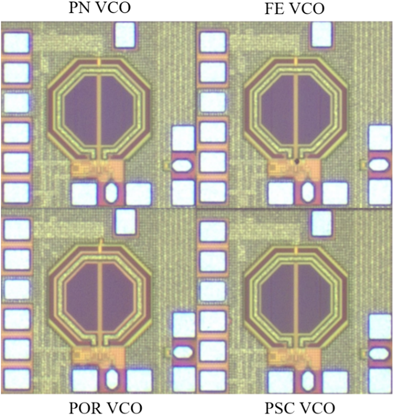
Figure 10. Photograph of the fabricated VCOs.
Inductors measurements
The inductors used for each type of VCO were put as stand-alone structures for measurements, to be able to assess the substrate resistivity’s impact on their quality factor at the targeted frequency band of 14–16 GHz and thus on the LC-tank of the VCOs. This was only done for the POR VCO’s inductor and the FE VCO’s inductor. Several dies were measured and very little variability was observed. The results are summarized in Fig. 11.
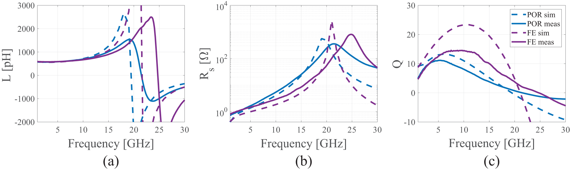
Figure 11. Measurement results of the inductors. (a) The inductance value l, (b) the series resistance  ${R_S}$, and (c) the inductor quality factor Q.
The results show the positive impact of the substrate resistivity on the quality factor of the inductors, which is significantly improved all over the region above 5 GHz. This happens not only because there are less losses in the substrate, but also because the HR version of the inductor is made using a stack of three thick metals from the FD-SOI technology, as described in the section “VCO design”, therefore reducing the inductor track’s series resistance.
Phase noise and tuning range measurements
The VCO core draws 7.2 mA from a 0.9 V voltage source (buffers draw 3.7 mA). The tuning range and phase noise of the VCOs were measured using the Keysight Signal Source Analyzer. The results are summarized in Fig. 12.
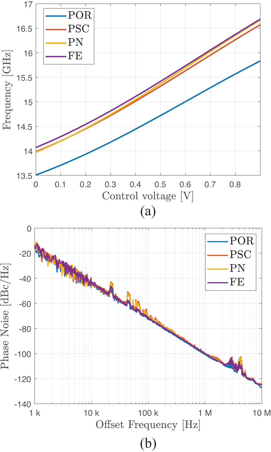
Figure 12. Measurement results of the tuning range and phase noise of the four VCOs. (a) Tuning range and (b) phase noise.
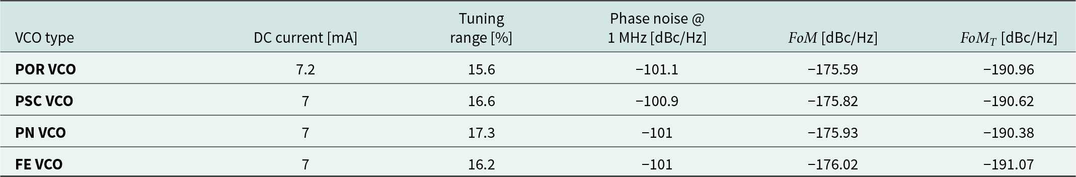
The figure highlights a shift of the oscillating frequency for the three VCOs meant for the HR substrate. This can be attributed not only to the different inductor designs having slightly different inductance values, but also different parasitic capacitance values as the layout of the two inductors is different. The POR VCO was measured on its intended POR wafer while the three other VCOs were measured on a different highly resistive wafer, this can also introduce variability in transistor bias points and therefore in the oscillation frequency of the VCO. All four VCOs achieve similar phase noise performance around −101 dBc/Hz @ 1 MHz offset. No significant improvement in phase noise is observed despite the higher quality factor of the inductors on HR substrates. Table 1 shows a summary of the four VCOs performance.
Table 1. Measured performance of the four VCOs designed
Substrate noise measurements
Regarding the main results of this work, the output spectrum of each VCO was measured with and without the injection of a 0 dBm power noise signal at varying frequencies. A 0 V bias was used for the FE passivation, which corresponds for this technology to minimal PSC-related substrate conduction (data not shown). Figure 13 shows the spectrum of the four VCOs when a 5 MHz continuous wave sinusoidal signal, representing substrate noise, is turned on and off. A spur appears in the vicinity of the fundamental signal at a 5 MHz offset frequency when the noise injection is turned on. Because of the non-linear behavior of the transistors in the VCOs, the noise signal mixes with the fundamental VCO signal, causing the spurs to appear. However, the spur power is 20 dB and 23 dB lower, respectively, for the PSC and the FE VCO, and completely disappears in the case of the PN VCO.

Figure 13. The output spectrum of the VCOs with and without the injection of a 0 dBm power 5 MHz frequency noise signal. (a) POR VCO, (b) PSC VCO, (c) PN VCO, and (d) FE VCO.
Additional measurements were performed by varying the frequency of the noise signal and the control voltage, which are summarized in Fig. 14. The tendency observed for all the frequencies in Fig. 14(a) is the same: an initial drop in the power of the noise spurs by more than 20 dB occurs when using an HR substrate, and an additional drop of around 6 dB is achieved when using the PN junction-passivated HR substrate and the FE-passivated HR substrate. This technique therefore seems to be more efficient than using guard rings around the active areas, as the latter shows a 25 dB spur reduction for a 900 MHz VCO but only 10 dB reduction for a 5.2 GHz VCO [Reference Checka, Wentzloff, Chandrakasan and Reif6].

Figure 14. Power of the first spur as a function of (a) VCO type and noise signal frequency  ${f_{noise}}$ at
  ${V_{ctrl}} = 0\,V$, (b) control voltage and VCO type at
  ${f_{noise}} = 40\,MHz$.
Figure 14(b) shows that for the POR VCO, the measured power of the spur caused by substrate noise coupling increases by 21 dB when increasing the control voltage from 0 V to 0.9 V, while it only increases by 10 dB for the PSC VCO, the PN VCO, and the FE VCO. These results highlight the important benefit of using HR substrates and suppressing PSC effects on the signal integrity of CMOS VCOs.
Conclusion
This paper investigates the effect of substrate resistivity on the spectral purity of a 14 GHz VCO fabricated in the 28 nm FD-SOI CMOS technology. The VCO was implemented on four substrate variants and measured under a substrate-injected, single-tone noise signal that creates spurs around the VCO fundamental frequency. Measurements show that implementing a VCO on an HR substrate reduces the substrate noise-generated spurs by more than 20 dB, and by 6 dB further when using a passivation technique such as the PN junctions or the FE passivation. These results highlight the important impact of substrate resistivity on the signal integrity of FD-SOI CMOS VCOs.
Competing interests
The author(s) declare none.

Youssef Bendou was born in Rabat, Morocco, in 1997. Starting 2015, he studied for 2 years under engineering preparatory classes in CPGE Moulay Youssef, Rabat, his hometown. He joined the Grenoble Institute of Technology, France, in 2017, to continue his engineering curriculum. He then enrolled in a M.S. degree in micro and nanotechnology for integrated systems, jointly delivered by l’École Polytechnique Fédérale de Lausanne (EPFL), Switzerland, the Politecnico di Torino (Polito), Italy, and Grenoble INP Phelma, France, in 2020. He is currently pursuing the Ph.D. degree with the Université catholique de Louvain, Belgium, in collaboration with the company STMicroelectronics in France, on the design of RF and mm-wave integrated circuits on the 28 nm FDSOI technology benefiting from the advantages of high-resistivity substrates.

Dimitri Lederer received the Electrical Engineering and Ph.D. degrees in applied sciences degree from the Université catholique de Louvain, Belgium, in 2000 and 2006, respectively. He then pursued post-doctoral studies at the Tyndall National Institute, Cork, Ireland where he worked on the fabrication and characterization of Si nanowires. From 2000 till 2006, he was a Research Assistant on the wideband characterization of advanced SOI material and devices for high-frequency applications. He joined the private sector in 2008 to develop electronics and microwave products for circa 15 years within the Research and Development teams of various small and large companies. From 2016 till 2020, he joined Global Foundries where he worked on the development of SOI-based technologies for microwave and mmWave applications (5G, 6G, IOT, automotive radars). He joined UCLouvain in 2020 as a Professor and conducts research in the field of THz technologies, devices and circuits. He is the owner of six patents and the author and co-author of more than 140 technical papers and conference contributions.

Andreia Cathelin received the degree in electrical engineering from the Polytechnic Institute of Bucharest, Bucharest, Romania, and the M.S. degrees from the Institut Supérieur d’Electronique du Nord (ISEN), Lille, France, in 1994, and the Ph.D. and “Habilitation à diriger des recherches” (French highest academic degree) degree from the Université de Lille 1, Villeneuve-d’Ascq, France, in 1998 and 2013, respectively. Since 1998, she has been with STMicroelectronics, Crolles, France, as the Advanced Research and Development Design Technical Director and a Technology Research and Development Fellow. She has authored or coauthored more than 150 technical papers and 14 book chapters, has co-edited the Springer book “The Fourth Terminal, Benefits of Body-Biasing Techniques for FDSOI Circuits and Systems” and has filed more than 40 patents.Her focus areas are in the design of RF/mmW/THz and ultralow-power circuits and systems. She is currently leading the RF Affinity team transversal inside the company, which enables knowledge creation and breakthrough solutions in the field toward open innovation and business impact. Dr. Cathelin is very active in the IEEE community since more than 15 years, strongly implied with SSCS and its Adcom (two terms up to 2022). She is a member of the VLSI Symposium Executive Committee. She is as well an active Founding Member of the IEEE SSCS Women in Circuits Group. She has been the TPC Chair of ESSCIRC 2020 and ESSCIRC 2021 in Grenoble, and the General Co-Chair of ESSCIRC-ESSDERC 2023 in Lisbon. She is also the IEEE RFIC Symposium TPC Member and has been for 10 years involved with ISSCC as the RF subcommittee chair and then a member of the Executive Committee. She has been a recipient and co-recipient of several awards with ISSCC and RFIC. She is also the winner of the 2012 STMicroelectronics Technology Council Innovation Prize, and has been awarded an Honorary Doctorate from the University of Lund, Sweden, promotion of 2020. She is currently an Associate Editor of IEEE TRANSACTIONS ON MICROWAVE THEORY AND TECHNIQUES and IEEE TRANSACTIONS ON CIRCUITS AND SYSTEMS—I: REGULAR PAPERS.

Jean-Pierre Raskin received the M.S. and Ph.D. degrees in applied sciences from Université catholique de Louvain (UCLouvain), Louvain-laNeuve, Belgium, in 1994 and 1997, respectively. In 1998, he joined the EECS Department of The University of Michigan, Ann Arbor, USA, for a postdoc of 2 years. In 2000, he joined the Microwave Laboratory of UCLouvain, Louvain-la-Neuve, Belgium, as an Associate Professor, and he has been a Full Professor since 2007. From September 2009 to September 2010, he was Visiting Professor at Newcastle University, Newcastle Upon Tyne, U.K. He is author or coauthor of more than 400 scientific journal articles. His research interests are the modeling, wideband characterization and fabrication of advanced SOI MOSFETs as well as micro and nanofabrication of MEMS/NEMS sensors and actuators, including the extraction of intrinsic material properties at nanometer scale. He is involved in the development of a more sustainable electronics. He has been managing a Chair of Excellence in eco-innovation at CEA-Leti since January 2024. He received the Médaille BLONDEL 2015, the SOI Consortium Award 2016, the European SEMI Award 2017, the Médaille AMPERE 2019, the Georges Vanderlinden Prize 2021 and the IET Achievement Medal in Electronics 2022, in recognition in his vision and pioneering work for RF SOI. He has been elected member of the Royal Academy of Belgium in 2023.


 Open access