


I. INTRODUCTION
With the entrance of many new wireless communication services in the new millennium, there will be a tremendous increase in the use of super wideband (SWB) printed monopole antennas (PMA), particularly owing to its low cost, small size, ease of fabrication, extremely wideband radiation characteristics, and omni-directional radiation pattern. To cater different services such as global positioning system (GPS), global system for mobile communications (GSM) 1800, the industrial, scientific and medical (ISM), wireless local area network (WLAN), ultra wideband (UWB) system, and satellite communication systems by the same devices, SWB printed monopole antennas will become more and more popular. Existing UWB [1] antenna can support limited number of wireless communication services and operates in the frequency band of 3.1–10.6 GHz with ratio bandwidth (RB) of 3.4:1. However, SWB antennas provide RB of more than 10:1. It was first supposedly reported by V. Rumsey in the late 1956, which was classified as a class of frequency independent antenna [Reference Rumsey2]. Currently a limited number of SWB printed monopole antennas have been proposed by the researchers across the globe [Reference Dorostkar, Islam and Azim3–Reference Chen, Sim and Row7]. In reference [Reference Dorostkar, Islam and Azim3], to enhance the bandwidth concept of circular hexagonal fractal antenna was utilized. The designed SWB antenna achieved RB of 20.4:1 with overall dimension of 45 × 31 × 1.57 mm3. Manohar et al. [Reference Manohar, Kshetrimayum and Gogoi4] designed tapered PMA (overall dimension of 30 × 40 × 1.6 mm3) with RB of 32:1 for voltage standing wave ratio (VSWR) ≤ 2.
In reference [Reference Liu, Esselle, Hay and Zhong5] Liu et al. developed an asymmetric SWB monopole antenna by using dual-branch feed network that provides large bandwidth (RB of 31:1) with overall dimension of 74 × 80 × 1.524 mm3. A semi-elliptical monopole antenna with overall dimension of 157.5 × 112.5 × 1.524 mm3 was presented in [Reference Yan, Zhong and Liang6] for SWB (RB of 19.7:1) applications. Chen et al. [Reference Chen, Sim and Row7] designed (size of 35 × 77 × 1.6 mm3) an egg shaped SWB monopole antenna with a bandwidth ratio greater than 12:1. Nevertheless, the major deficiencies of the above stated antennas are large volume and not easy to accommodate with the limited space provided by the future hand-held gadgets.
Unfortunately, one important issue to be noted for SWB antenna is that, it may cause electromagnetic interference to the existing narrow band WLAN operating in 5.15–5.35 GHz and 5.725–5.825 GHz bands. These narrow bands lie within the SWB band. To mitigate this interference issue, we have proposed SWB antennas with band-notched characteristics. In the last few years, several band-notched antennas have been reported by researchers across the globe [Reference Cho, Kim, Choi, Lee and Park8–Reference Ojaroudi, Ghobadi and Ojaroudi13]. But to author's knowledge, there are no band-notched SWB antennas reported in the literature.
In this communication, we propose a compact antenna structure for realization of SWB radiation characteristics along with notch capability. Here we demonstrate that by employing the triangular tapered feed line for the radiating patch, wider impedance bandwidth can be achieved. By cutting rectangular slots with same dimension on two sides of the partial ground plane, wider impedance bandwidth (frequency band of 0.9–100 GHz) of the proposed SWB antenna can be achieved. Proposed SWB antenna can achieve all critical requirements like SWB radiation characteristics, bandwidth and size reduction compared with the existing SWB antennas [Reference Dorostkar, Islam and Azim3–Reference Yan, Zhong and Liang6]. Further not to affect the band from 5 to 6 GHz used in WLAN we introduce appropriate notches at this frequency. We have used C-shaped parasitic element as well as two L slots etched in the ground plane similar to what have been reported in [Reference Li, Hei, Feng and Shi10, Reference Sarkar, Srivastava and Saurav11]. The proposed antenna is very promising for various modern communication applications such as GSM1800 (1.71–1.88 GHz), personal communications service (PCS) (1.85–1.99 GHz), advanced wireless service (AWS)-3 (2.155–2.175 GHz), wireless communications service (WCS) (2.345–2.360 GHz), ISM (2.402–2.480 GHz), multichannel multipoint distribution service (MMDS) (2.500–2.690 GHz), UWB (3.1–10.6 GHz) and UWB vehicular radar (22–29 GHz). Due to extremely large bandwidth, the proposed SWB antenna may be used for spectrum sensing in cognitive radio [Reference Grayaver14]. The antennas were designed and optimized successfully using frequency domain three-dimensional (3D) full wave electromagnetic solver High Frequency Structure Simulator (HFSS) version 14.
II. ANTENNA CONFIGURATION
Figure 1 shows the schematic diagram of the proposed band-notched SWB monopole, which is printed on RT/Duroid 5870 substrate with a thickness (h) of 0.787 mm and a dielectric constant of 2.23 and a loss tangent of 0.0009. Proposed SWB monopole antenna structure composed of a tapered radiating patch, tapered feed region which is fed by a 50 Ω triangular tapered feed line, and printed on a chamfered ground plane (CGP). Here all four parts of the proposed antenna is optimized to get large bandwidth as well as size reduction. To create the band-notched characteristics for WLAN, a C-shape parasitic element is employed, which is electromagnetic coupled to the radiating patch. To further improve the notching characteristics of the proposed antenna, two symmetrical L-slots have been placed in the CGP. To design the proposed band-notched SWB antenna we have chosen RT/Duroid substrate instead of FR4 substrate, especially for very high frequencies or millimeter wave frequencies. FR4 substrate becomes quite lossy at higher frequencies unlike RT/Duroid substrate [Reference Huang and Boyle15]. The optimal dimensions of the proposed antennas are as follows: L = 40 mm, W = 30 mm, H = 22 mm, M = 22 mm, l f = 7 mm, W g = 7 mm, l n = 11 mm, l K = 5 mm, W K = 8 mm, R 1 = 22.7 mm, R 2 = 3.05 mm, l y = 3 mm, l C = 8 mm, W m = 4 mm, l m = 1 mm, p = 1 mm, N = 15 mm, B = 3 mm, T = 0.8 mm, W d = 10 mm, W h = 9.5 mm, Q = 60°, l d = 9 mm, l g = 4 mm, l s = 4 mm, F = 6.7 mm, R = 6.2 mm, K = 6.8 mm, G = 0.8 mm, A = 3 mm, V = 7 mm.
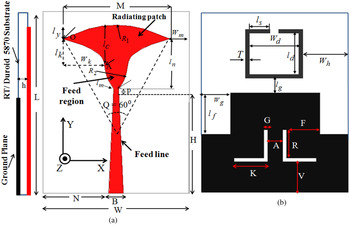
Fig. 1. Geometry of the proposed band-notched SWB monopole antenna; (a) front view and (b) back view.
III. ANTENNA DESIGN CONCEPT
In this section, first we will explore about SWB PMA which covers the frequency range from 0.9 to 100 GHz. Then the band-notched functionality will be discussed (Table 1).
Table 1. Comparison of the antenna size, RB, and peak gain of the proposed band-notched SWB PMA to band-notched UWB PMA.

A) Methodology to achieve SWB
In the present antenna configuration i.e. Fig. 1, a feed region connection, between the feed line and, then radiating patch, was brought in to improve the antenna's performance. Due to optimal tapered [Reference Raicu16] (Raicu's universal taper) connections between the feed line and the main patch, broad impedance bandwidth is obtained. The triangular tapered feed line is also used in order to improve the impedance matching. Moreover, it could be noticed that chamfered ground structures (CGS) i.e. two symmetrical rectangular slot cuts in partial ground plane are also responsible for the wider impedance bandwidth of 0.9–100 GHz (bandwidth ratio of 111.1:1) except in the notched band of 4.7–6 GHz. To get the length of the tapered line (l p = H + p), method reported in [Reference Manohar, Kshetrimayum and Gogoi4] is followed. If Z L and Z 0 be the antenna load impedance and characteristic impedances of the feed line, then the impedance function of triangular tapered feed line is obtained from the equation given below [Reference Collin17, Reference Pozar18]
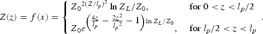 $$Z(z) = f(x) = \left\{ {\matrix{ {{Z_0}^{2{{(Z/{l_p})}^2}} \ln {Z_L}/{Z_{0}},}\hfill & {{\rm for}\;0 \lt z \lt {l_p}/2}\hfill \cr {{Z_0}{e^{\left(\textstyle{{{4z} \over {{l_p}}} - {{2{z^2}} \over {{l_p}^2 }} - 1} \right)\ln {Z_L}/{Z_{0}}}},\;}\hfill & {{\rm for}\;{l_p}/2 \lt z \lt {l_p}} \cr }\hfill } \right..$$
Relating this impedance function to Γ (θ) function will result in equation (2). A closed form solution of the Riccati equation for triangularly tapered feed line is given in [Reference Collin17]
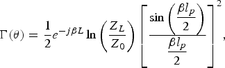 $${\rm \Gamma (}\theta {\rm )} = \displaystyle{1 \over 2}{e^{ - j\beta L}}\ln \left( {\displaystyle{{{Z_L}} \over {{Z_0}}}} \right){\left[ {\displaystyle{{\sin \left( {\displaystyle{{\beta {l_p}} \over 2}} \right)} \over {\displaystyle{{\beta {l_p}} \over 2}}}} \right]^2},$$
where Γ (θ) is the reflection coefficient, β is the phase constant and l p is the triangular tapered feed line length. In designing the radiating patch, an elliptical curve has been employed for the design of main patch depicted in Fig. 1. The quarter elliptical arcs begin with the x and y radius and ends with the elliptical arc. The arc length of the quarter elliptical can be obtained by
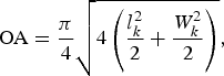 $${\rm OA} = \displaystyle{\pi \over 4}\sqrt {4\left( {\displaystyle{{l_k^2} \over 2} + \displaystyle{{W_k^2} \over 2}} \right)},$$
where OA is the perimeter of the quarter ellipse and the value of OA = 10.5 mm with l k and W k as the minor and major radius. To get the SWB antenna behavior, there are many parameters that have been optimized, which can affect the impedance matching characteristics of the proposed antenna. Figure 2 demonstrates the simulated return loss for the proposed monopole antenna design of Fig. 1(a) with and without defected ground structures (DGS). It can be seen that in the absence of DGS, the behavior of |S 11| > −10 dB at frequency band (3.5–6.5 GHz). By placing two slots in the ground plane it can be observed that the slots can adjust the electromagnetic coupling effects between the monopole and the ground plane and improve its impedance bandwidth across the whole spectrum as shown in the Fig. 2. Figure 3 depicts the simulated return loss for the proposed monopole antenna with various circular arc angle (Q). When the circular arc angle (Q) increases from 60° to 65°, approximate wide impedance bandwidth is provided between 0.9 and 47 GHz, however impedance matching becomes worse between 47 and 53 GHz. As Q = 60°, the super wide impedance bandwidth is achieved from 0.9 to 100 GHz. While, circular arc angle (Q) decreases from 60° to 55°, |S 11| > −10 dB between (82–87 GHz and 90–95 GHz).

Fig. 2. Simulated return loss for the proposed SWB antenna with and without CGS.

Fig. 3. Simulated return loss for the proposed SWB antenna with various circular arc angles (Q).
B) Study of band-notched function design
Band-suppression characteristic over the whole interference band is realized by the C-shape parasitic element in the back plane of the substrate, which is electromagnetically coupled to the main patch. The C-shape parasitic element acts as a half-wave resonant structure and can perturb the current distribution at certain frequency band (4.7–6 GHz), where the band-notched characteristics of the antenna are expected. Further increasing the strong rejection at the band-notch region (4.7–6 GHz) two symmetrical L-slots are etched with CGS. Band-notched characteristics can be achieved by tuning the parameters W d , ld, T, and l s . A dimension of the C-shaped parasitic elements is selected according to the following expression
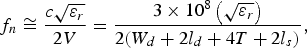 $${f_n} \cong \displaystyle{{c\sqrt {{\varepsilon _r}}} \over {2V}} = \displaystyle{{3 \times {{10}^8}\left( {\sqrt {{\varepsilon _r}}} \right)} \over {2({W_d} + 2{l_d} + 4T + 2{l_s})}},$$
where V is the physical length of C-shape parasitic element and f n is the corresponding band-notch frequency (5.35 GHz). W d , l d , and T is the width, length, and thickness of C-shape parasitic element. Figure 4 demonstrates the simulated surface current distribution for the proposed monopole antenna at the band-notched center frequency of 5.35 GHz. It can be seen that current flows on the C-shape parasitic element are more egregious around notch frequency and they are opposite in direction (out-of-phase) to the current flow on the main patch, which can easily cancel out the radiated field and offers strong attenuation near the notched frequency and makes it as a non-responsive antenna at the notch frequency of 4.7–6 GHz. To understand more about antenna characteristics on the band-notched portion, we change one parameter at a time, fixing the others. Figure 5 exhibits the simulated return loss of various values of length l d of the C-shape parasitic element. The values of l d are varied from 8 to 10 mm. In this arrangement, center of the notched frequency changes from 5.35 to 5.8 GHz as l d changes from 9 to 8 mm. Rejection band is tuned at l d = 9 mm. The simulated return loss for different values of T for C-shape parasitic element is plotted in Figure. 6. It is observed for T value greater than 0.8 mm the notch frequency shifts 0.6 GHz lower to band-notch frequency.

Fig. 4. Simulated current distribution at notch frequency 5.35 GHz.
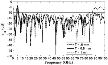
Fig. 5. Simulated return loss for the proposed band-notched SWB antenna with different arm width (T).

Fig. 6. Simulated return loss for the proposed band-notched SWB antenna with different arm length (l d ).
However, by decreasing the value of T from 0.8 to 0.6 mm center of the notched frequency decreases by 0.4 GHz. The optimum value of T is taken as 0.8 mm. The simulated reflection coefficient versus the operating frequency for different widths W d of the C-shape parasitic element is plotted in Fig. 7. It can be seen that for W d values smaller than 10 mm notch frequency shifts 1 GHz higher the band-notch region and provide much wider notch characteristics i.e. 4.7–7 GHz. This wide notch-band unnecessarily blocks usable frequencies from 6 to 7 GHz. However, when the width (W d ) of the C-shape parasitic element increases from 10 to 11 mm notched frequency decreases. We have also designed equivalent circuit model [Reference Telzhensky and Leviatan20] for the band-notched SWB antenna as shown in Fig. 8. In this model SWB impedance characteristics can be achieved due to several resonances excited by the SWB antenna and each resonance can be modeled as a parallel RLC circuit [Reference Telzhensky and Leviatan20], while the band-notched portion is modeled as a series LC circuit.
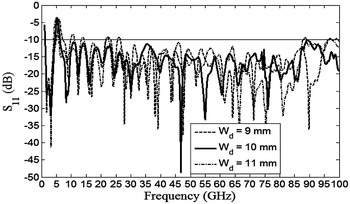
Fig. 7. Simulated return loss for the proposed band-notched SWB antenna with different arm width (w d ).
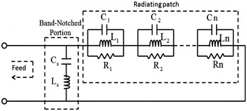
Fig. 8. Equivalent circuit model of the proposed band-notched SWB PMA.
VI. SIMULATION AND EXPERIMENTAL RESULTS
In order to validate the results of the proposed band-notched SWB antenna, first we have simulated the proposed antenna using HFSS in both frequency and time domain and then compared with measured results.
A) Frequency domain performance
The photograph of the fabricated antenna is shown in Figure. 9. It is simulated with the 3D electromagnetic simulation software HFSS and measured with vector network analyzer (Agilent ZVA 24). Figure 10 shows simulated and measured return loss of the proposed band-notched SWB antenna. From the Fig. 10 it is observed that the antenna provides broadband performance (frequency bandwidth from 1 to over 25 GHz) with band-notch from 4.7 to 6 GHz. Figure 11 displays three far-field radiation patterns in the E-plane and H-plane at three different frequencies (a) 3.1 GHz, (b) 10 GHz, and (c) 20 GHz. The proposed antenna has a nearly omni-directional pattern and low cross-polarization level in the H-plane radiation pattern at frequencies 3.1 and 10 GHz. E-plane radiation patterns shows a typical bidirectional (figure- of-eight) at frequencies 3.1 and 10 GHz. However, at frequency 20 GHz, antenna generates multi-nulls in the E-plane and H-plane and also the cross-polarization level increases with higher frequencies. Overall the proposed SWB monopole antenna exhibit approximately stable radiation patterns and behaves similarly to the typical planar monopole antennas. Figure 12 presents the measured and simulated peak gain with and without parasitic element for the proposed band-notched SWB antenna. It is found that the measured antenna gain is about −2 dBi at 1 GHz. It increases with frequency and attains 7 dBi at 25 GHz. Antenna gain decreases abruptly at the center frequency of 5.35 GHz, which shows appropriate band-notch for coexistence with WLAN appliances.
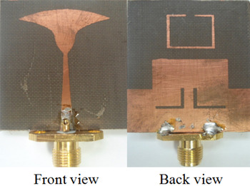
Fig. 9. Photograph of the fabricated prototype band-notched SWB antenna.
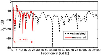
Fig. 10. Measured and simulated return loss for the proposed band-notched SWB monopole antenna.

Fig. 11. Simulated and measured radiation pattern for the proposed band-notched SWB antenna (red color: simulation, black color: experimental, solid line: co-polar and dashed line: cross-polar).

Fig. 12. Measured and simulated peak gain for the proposed band-notched SWB monopole antenna.
B) Time domain performance
In order to comprehend the time-domain analysis, two identical antennas were utilized as transmitter and receiver. They are separated by a distance of 60 cm and kept at three different orientations 0°, 45°, and 90°. Figures 13 and 14 shows the fifth-order-derivative Gaussian input pulse waveform in time domain and its power spectral density (dBm/MHz) with reference to federal communications commission (FCC) mask. To verify the FCC spectral mask for indoor systems, the antenna is assumed to be excited by the UWB signal as suggested in [21].
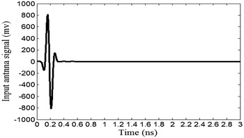
Fig. 13. Fifth-order-derivative Gaussian input.

Fig. 14. Power spectral density.
This UWB signal is the fifth derivative of the Gaussian pulse and is given by (5)
 $${G_5}(t) = A\left( { - \displaystyle{{{t^5}} \over {\sqrt {2\pi} {\sigma ^{11}}}} + \displaystyle{{10{t^3}} \over {\sqrt {2\pi} {\sigma\, ^9}}} - \displaystyle{{15t} \over {\sqrt {2\pi} {\sigma ^7}}}} \right).{\rm exp}\left( { - \displaystyle{{{t^2}} \over {2{\sigma ^2}}}} \right).$$
Here, C is a constant that can be chosen to comply with peak power spectral density that the FCC will permit. σ has to be 51 ps to ensure that the shape of the spectrum complies with the FCC spectral mask. Figure 15 shows the measured receiving antenna signal for the proposed band-notched antenna with different orientations, i.e. θ = 0°, 45°, and 90°. Ringing distortion has been observed in the received signal as shown in Fig. 15. At 0° orientation, received signal amplitude is 320 mV. However at 45° and 90° orientations, received signals amplitude are 300 and 200 mV, respectively.

Fig. 15. Measured receiving antenna signals for the proposed band-notch antenna with different orientations θ = 0°, 45°, and 90°.
V. CONCLUSION
A compact band-notched printed SWB monopole antenna has been proposed and extensively investigated in this paper. We have used triangular tapered feed line for broadband matching. In the feed region, we have used Raicu's universal taper for best and optimal taper. Thereby we can achieve SWB impedance matching from 0.9 to 100 GHz (bandwidth ratio of 111.1:1), except in the notched band of 4.7–6 GHz. With proper and simple C-shaped parasitic element integrated with ground plane, a band-notched performance from 4.7 to 6.0 GHz can be achieved. It helps in coexistence of SWB communication with WLAN devices. Both these devices can be deployed in the same area without any interference. The designed antenna has a simple configuration and compact in size compared with conventional structure.
 Murli Manohar was born in Bhagalpur, India in 1984. He received his M.Tech. degree in Electronics Communication and System from the National Institute of Technology Rourkela, India in 2010 and the Ph.D. degree from the department of Electronics and Electrical Engineering, Indian Institute of Technology Guwahati in 2015. Since 2014, he is working as a faculty member at the department of Electronics and Communication Engineering, National Institute of Technology Goa. His main research area is in antenna and RF engineering with focus on SWB printed monopole antennas.
 Rakhesh Singh Kshetrimayum received his Ph.D. degree from the School of Electrical and Electronic Engineering (EEE), Nanyang Technological University (NTU) Singapore in 2005. Since 2005, he has been with the department of EEE, IIT Guwahati as an Associate Professor (2010), Assistant Professor (2006–2010) and Senior Lecturer (2005–2006). He worked as a Postdoctoral Scholar at the department of EE, Pennsylvania State University (PSU) USA (2005), Research Associate Provisional at the department of Electrical Communication Engineering (ECE), Indian Institute of Science (IISc) Bangalore (2004–2005), Teaching Assistant at the School of EEE, NTU Singapore (2002–2003) and Trainee Software Engineer at Mphasis Pune, India (2000–2001). Dr. Kshetrimayum is the recipient of SEFOGG Young Engineer Award (2011), Department of Science & Technology India (SERC) Fast Track Scheme for Young Scientists (2007–2010) and NTU Research Scholarship from 2001 to 2004. His current areas of research interests are in printed antennas and circuits, UWB communications, and MIMO wireless communications. He has been involved in organizing several IEEE international conferences as Technical program chair/co-chair, Publication chair, Program chair, Session chair and Technical program committee. He is the Editor-in-Chief of Inderscience journal International Journal of Ultra Wideband Communications and Systems. Since 2014, he is a Fellow of the Institution of Electronics and Telecommunication Engineers (IETE), India, Optical Society of India (OSI) and Antenna Test & Measurement Society (ATMS), India and a senior member of the Institute of Electrical and Electronics Engineers (IEEE), USA. He is also a senior member of the International Association of Computer Science and Information Technology (IACSIT), Singapore and a member of Applied Computational Electromagnetics Society (ACES), USA and European Microwave Association (EuMA), Belgium.
 Anup Kumar Gogoi is a Professor of Electronics and Electrical Engineering and Dean of outreach education programme at the Indian Institute of Technology Guwahati. He received his Ph.D. degree from the Department of Electrical Engineering, Indian Institute of Technology Kanpur. His areas of research interests are in Electromagnetics, Microwave Engineering, RF circuits and Systems Design.


